VITESSE
SEMICONDUCTOR CORPORATION
Data Sheet
High Performance Serial
Backplane Transceiver
VSC870
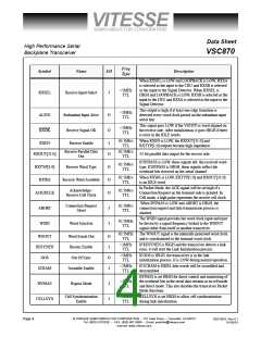
Freq
I/O
Symbol
Name
Description
Type
When RXSEL is LOW and LOOPBACK is LOW, RXSA
is selected as the input to the CRU and RXSB is selected
as the input to the Signal Detector. When RXSEL is
HIGH and LOOPBACK is LOW, RXSB is selected as the
input to the CRU and RXSA is selected as the input to the
Signal Detector.
<1MHz
TTL
RXSEL
Receive Input Select
I
This output is high if at least one edge transition is
detected every word clock period on the redundant input
serial line.
<1MHz
TTL
ALIVE
RXOK
Redundant Input Alive
O
O
This signal goes LOW if the VSC870 is word aligned on
the receive side. After initialization, it goes HIGH if there
is error in the IDLE words.
<1MHz
TTL
Receive Signal OK
Receive Enable
62.5Mb/s
TTL
When RXEN is LOW, the RXOUT[31:0] and
RXTYP[1:0] outputs become high impedance.
RXEN
I
Receive Parallel Data
Out
62.5Mb/s
TTL
RXOUT[31:0]
O
32-bit parallel data output for the receive side.
If BYPASS is LOW, these signals tell the received word
type. If BYPASS is HIGH, these signals reflect the
overhead bits received on the serial channel.
62.5Mb/s
TTL
RXTYP[1:0]
RXWA
Receive Word Type
O
O
O
62.5Mb/s
TTL
When RXWA is LOW, RXTYP[1:0] and RXOUT[31:0]
is an IDLE word.
Receive Word Available
In Packet Mode, the ACK signal will be set high if a
Connection Request on the transmit side is granted. In
Cell mode, a high pulse represents the receive cell clock.
Acknowledge /
Receive Cell Clock
62.5Mb/s
TTL
ACK/RCLK
When BYPASS is LOW and ABORT is HIGH, the
connection request and data transmission process is
aborted.
Connection Request
Abort
62.5Mb/s
TTL
ABORT
WSIN
I
I
The WSIN signal provides the word clock input and must
be driven by a signal frequency locked to the WSOUT
signal either from itself or another transceiver.
62.5MHz
TTL
Word Synch In
62.5MHz
TTL
The WSOUT signal is the internally generated word clock
and is synchronized to the transmit word clock.
WSOUT
RESYNEN
OOS
Word Synch Out
Resync Enable
Out Of Sync
O
I
<1MHz
TTL
If RESYNEN is HIGH and the transceiver detects a link
error, it will start the Link Initialization process.
<1MHz
TTL
If OOS is HIGH, the transceiver is in the link
initialization process. It is LOW during normal operation.
O
I
<1MHz
TTL
If SCRAM is HIGH, data words will be scrambled and
descrambled.
SCRAM
Scramble Enable
BYPASS is set HIGH for direct control and monitoring of
the overhead bits in the serial data streams as in cell mode
and direct mode. This also disables the transceiver Packet
Mode functions.
<1MHz
TTL
BYPASS
Bypass Mode
I
I
Cell Synchronization
Enable
<1MHz
TTL
CELLSYN is set HIGH to allow cell synchronization
during link initialization.
CELLSYN
© VITESSE SEMICONDUCTOR CORPORATION • 741 Calle Plano • Camarillo, CA 93012
Tel: (800) VITESSE • FAX: (805) 987-5896 • Email: prodinfo@vitesse.com
Internet: www.vitesse.com
Page 4
G52190-0, Rev 4.1
01/05/01

 VITESSE [ VITESSE SEMICONDUCTOR CORPORATION ]