VITESSE
SEMICONDUCTOR CORPORATION
Data Sheet
High Performance Serial
Backplane Transceiver
VSC870
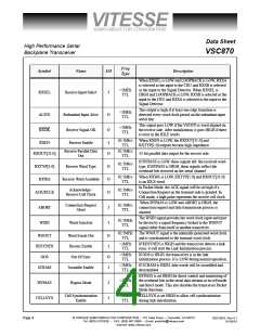
Freq
I/O
Symbol
Name
Description
Type
If BYPASS is LOW, this signal can be set HIGH to enable
REN delay mode. In Cell Mode, DLYEN/CCKIN can be
used as an input for cell clock alignment.
DLYEN/
CCKIN
Delay Enable/Cell Clock
Input
<1MHz
TTL
I
<1MHz
TTL
When this signal is HIGH, the serial input is looped back
to the serial output. It should be normally set LOW.
FACLPBK
WCLK
Facility Loopback
Word Clock
I
62.5MHz
TTL
O
The word clock is a delayed version of the WSIN signal.
A 62.5 MHz local reference clock that is used to keep the
CRU close to the incoming bit clock frequency before the
alignment process begins. Is also used as a reference
clock for the CMU.
62.5MHz
TTL
REFCLK
Local Reference Clock
I
<1MHz
TTL
RESET
Reset
I
I
Global chip reset (active HIGH).
When TESTEN is HIGH, the REFCLK is used in place
of the bit clock for low speed testing. Used for ATE
testing only. Set to logic LOW during normal operation.
<1MHz
TTL
TESTEN
Scan Test Enable
62.5Mb/s
TTL
LTIME is set HIGH to use the recovered bit clock for the
transmit side.
LTIME
VSCTE
Loop Time Mode
I
I
<1MHz
TTL
Used for ATE testing of the parametric NOR chain in the
I/O frame. Set to logic LOW during normal operation.
NOR Chain Test Enable
VDDA
VSSA
CMU Power Supply
CMU Ground
P
P
3.3V
0V
Clean power supply for CMU
Clean ground for CMU
© VITESSE SEMICONDUCTOR CORPORATION • 741 Calle Plano • Camarillo, CA 93012
Tel: (800) VITESSE • FAX: (805) 987-5896 • Email: prodinfo@vitesse.com
Internet: www.vitesse.com
G52190-0, Rev 4.1
01/05/01
Page 5

 VITESSE [ VITESSE SEMICONDUCTOR CORPORATION ]