VITESSE
SEMICONDUCTOR CORPORATION
Data Sheet
High Performance Serial
Backplane Transceiver
VSC870
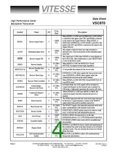
Functional Description
The VSC870 transceiver can be used in one of the three operation modes: Packet Mode, Cell Mode and Direct
Mode. In Packet mode, the VSC870 is intended to work in conjunction with the VSC880 switch chip to provide a self
routing switching system and to support variable length data packets. In Cell Mode, the transceiver works in
conjunction with the VSC880 switch chip to provide a cell synchronized switching system. In this mode, it can
support only fixed length data packets (cells), and routing decisions are carried out in a user defined controller chip
and synchronized to a cell clock. In Direct mode, the VSC870 can connect to other transceivers to provide a high
bandwidth serial backplane data link.
The following sections give a detailed description of generic features which are provided in all three modes,
followed by the operation of the transceiver in each mode. Most of the discussions in this data sheet include some of
the switch chip functions (see the VSC880 data sheet).
1.0 Common Features
1.1 Synchronization
1.1.1 Link Characteristic
The serial link is used to connect the transceivers to the switch chip or to other transceivers. These links operate
at 2.125Gb/s and are initialized simultaneously at power up, or separately when a link error occurs. A link is first bit
synchronized, then word synchronized and, if CELLSYN is HIGH, cell synchronized. In Packet or Cell mode, the
switch acts as the master, generating the bit clock along with the word and cell boundary information. The
transceivers act as slaves, recovering the bit clock, word clock and cell clock. In Direct mode, the transceivers can be
configured as either masters or slaves using the MODE[1:0] signals, with the masters generating the bit and word
clocks. The transceiver also contains redundant serial inputs and outputs which can be used with a redundant switch
chip or redundant transceiver.
1.1.2 Data Scrambling
A 15% edge transition density must be guaranteed on the serial data links for the CRU to work properly. All
command words and connection request words contain this required density. In order to get this density on data
words, scrambling is employed. If SCRAM is set HIGH, the 32-bit data words are scrambled in the transmitter and
de-scrambled in the receiver with a (1+X1+X7) pattern to guarantee high transition density. This is the same pattern
used in SONET scrambling. In all operating modes, data words are recognized by TXTYP[1:0] = 01 or 10. Words
such as the connection request and header word in Packet Mode or cell clock in Cell Mode or the IDLE word in
Direct Mode are used to initiate the scrambling pattern. If the user can guarantee edge densities greater than or equal
to 15%, scrambling can be turned off by setting SCRAM = LOW.
1.1.3 Bit Synchronization
In Packet and Cell Mode, the switch acts as the source of the bit clock. It multiplies the local 62.5MHz word
clock by 34 to generate a 2.125GHz clock, and uses this clock to serialize the 32-bit data word and 2 overhead bits.
© VITESSE SEMICONDUCTOR CORPORATION • 741 Calle Plano • Camarillo, CA 93012
Tel: (800) VITESSE • FAX: (805) 987-5896 • Email: prodinfo@vitesse.com
Internet: www.vitesse.com
Page 6
G52190-0, Rev 4.1
01/05/01

 VITESSE [ VITESSE SEMICONDUCTOR CORPORATION ]