VITESSE
SEMICONDUCTOR CORPORATION
Data Sheet
High Performance Serial
Backplane Transceiver
VSC870
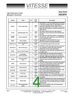
Package Pin Descriptions
Freq
Type
Symbol
Name
I/O
Description
62.5Mb/s
TTL
TXIN[31:0]
Transmit Parallel Data In
I
32-bit parallel data input for the transmit side.
If BYPASS is LOW, these signals designate the transmit
word type. If BYPASS is HIGH, these signals directly
control the overhead bits sent on the serial channel.
62.5Mb/s
TTL
TXTYP[1:0]
TXEN
Transmit Word Type
Transmit Enable
I
I
When TXEN is HIGH, TXIN[31:0], TXTYP[1:0] are
loaded in to the transceiver on the next WCLK. When
TXEN is LOW, the transceiver ignores TXIN[31:0] and
TXTYP[1:0] and sends IDLE words at the serial output.
62.5Mb/s
TTL
When RTR is HIGH, the receiving side memory system is
ready to receive data. If LOW, it sends a back pressure
(flow control) signal to the source port card telling it to
stop sending data. In Cell Mode, set RTR LOW to cell
synchronize to the external cell clock. If RTR is HIGH,
cell clock is recovered from the bit stream.
62.5Mb/s
TTL
RTR
Ready To Receive
I
In Packet Mode, when BYPASS is LOW, RTM/TCLK is
set HIGH at the beginning of each data transmission and
set LOW when the data packet has been successfully sent
to all outputs. In Cell Mode, a HIGH pulse represents the
transmit cell clock.
Retransmit Mode/
Transmit Cell Clock
62.5Mb/s
TTL
RTM/TCLK
O
When BYPASS is LOW, RFM is set HIGH whenever a
retransmission of data is required due to contention for
destination ports.
62.5Mb/s
TTL
RFM
Read From Mark
Transmit signal OK
Read Enable
O
O
O
This signal is LOW if MODE[1] is HIGH and the
transceiver is word aligned on the transmit side. After
initialization it will go HIGH for one word clock if there
is a cell clock error.
<1MHz
TTL
TXOK
When REN is HIGH, the transceiver is ready to read data
at TXIN[31:0] and TXTYP[1:0]. This signal can be
forced low by the received flow control signal.
62.5Mb/s
TTL
REN
<1MHz
TTL
These mode control pins are used to configure link
synchronization. See Section 1.5.
MODE[1:0]
Mode Control
Transmit Serial Output A
Transmit Serial Output B
Loop Back
I
O
O
I
TXSA+/
TXSA-
2.125Gb/s
LVDS
High speed serial differential transmit channel A
High speed serial differential transmit channel B
TXSB+/
TXSB-
2.125Gb/s
LVDS
<1MHz
TTL
When LOOPBACK is HIGH, the CRU and signal
detector select the serial data output channel as an input.
LOOPBACK
RXSA+/
RXSA-
2.125Gb/s
LVDS
Receive Serial Input A
Receive Serial Input B
I
High speed serial differential receive channel A
High speed serial differential receive channel B
RXSB+/
RXSB-
2.125Gb/s
LVDS
I
© VITESSE SEMICONDUCTOR CORPORATION • 741 Calle Plano • Camarillo, CA 93012
Tel: (800) VITESSE • FAX: (805) 987-5896 • Email: prodinfo@vitesse.com
Internet: www.vitesse.com
G52190-0, Rev 4.1
01/05/01
Page 3

 VITESSE [ VITESSE SEMICONDUCTOR CORPORATION ]