VSC8601 Datasheet
Pin Descriptions
6.2
Pins by Function
This section contains the functional pin descriptions for the VSC8601 device. The
following table contains notations for definitions of the various pin types.
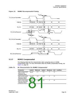
Table 78.
Pin Type Symbols
Symbol
Pin Type
Description
I
Input
Input with no on-chip pull-up or pull-down resistor.
I/O
Input and Output
Input and output signal with no on-chip pull-up or
pull-down resistor.
IPU
IPD
Input with pull-up
Input with on-chip 100 kΩ pull-up resistor to VDDIO.
Input with on-chip 100 kΩ pull-down resistor to VSS.
Input with pull-down
IPD/O
Bidirectional with
pull-down
Input and output signal with on-chip 100 kΩ pull-down
resistor to VSS.
I
PU/O
Bidirectional with
pull-up
Input and output signal with on-chip 100 kΩ pull-up
resistor to VDDIO or VDD33.
O
Output
Output signal.
OZC
Impedance controlled
output
Integrated (on-chip) source series terminated, output
signal.
OD
OS
Open drain
Open drain output.
Open source
Open source output.
ADIFF
ABIAS
IA
Analog differential
Analog bias
Analog differential signal pair for twisted pair interface.
Analog bias pin.
Analog input
Analog Input for sensing variable voltage levels.
IPU5V
Input with pull-up
Input with on-chip 100 kΩ pull-up resistor to VDD33.
These pins are 5 V tolerant.
OCRYST
NC
Crystal output
No connect
Crystal clock output pin. If not used, leave unconnected.
No connect pins must be left floating.
6.2.1
Twisted Pair Interface
The following table lists the device pins associated with the device two-wire, twisted
pair interface.
Table 79.
Twisted Pair Interface Pins
Pin
53
54
55
56
58
59
60
61
Name
TXVPA
TXVNA
TXVPB
TXVNB
TXVPC
TXVNC
TXVPD
TXVND
Type
ADIFF
ADIFF
ADIFF
ADIFF
ADIFF
ADIFF
ADIFF
ADIFF
Description
TX/RX channel A positive signal
TX/RX channel A negative signal
TX/RX channel B positive signal
TX/RX channel B negative signal
TX/RX channel C positive signal
TX/RX channel C negative signal
TX/RX channel D positive signal
TX/RX channel D negative signal
Revision 4.1
September 2009
Page 85

 VITESSE [ VITESSE SEMICONDUCTOR CORPORATION ]