VSC8601 Datasheet
Electrical Specifications
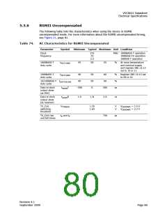
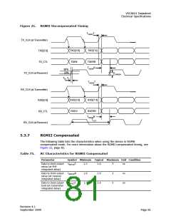
Figure 21.
RGMII Uncompensated Timing
TSKEW
T
TX_CLK (at Transmitter)
TXD[3:0]
TXD[3:0]
TXEN
TXD[7:4]
TXERR
TX_CTL
TSKEW
R
80%
20%
TX_CLK (at Receiver)
VTHRESH
TR, TF
TSKEW
T
RX_CLK (at Transmitter)
RXD[3:0]
RXD[3:0]
RXDV
RXD[7:4]
RXERR
RX_CTL
TSKEW
R
TCYC
RX_CLK (at Receiver)
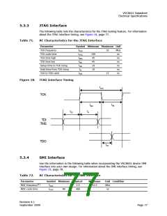
5.3.7
RGMII Compensated
The following table lists the characteristics when using the device in RGMII
compensated mode. For more information about the RGMII compensated timing, see
Figure 22, page 82.
Table 75.
AC Characteristics for RGMII Compensated
Parameter
Symbol Minimum Typical Maximum Unit Condition
Data to clock output
setup (at PHY
integrated delay)
t
SETUPT
1.2
1.0
1.2
2.0
2.0
2.0
3
3
3
ns
ns
ns
Data to clock output
setup (at receiver
integrated delay)
tSETUPR
Data to clock output
hold (at transmitter
integrated delay)
tHOLDT
Revision 4.1
September 2009
Page 81

 VITESSE [ VITESSE SEMICONDUCTOR CORPORATION ]