VSC7961
Data Sheet
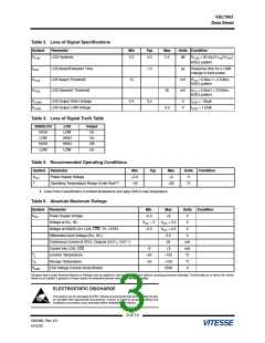
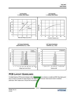
LOS Sensitivty
LOS Hysterisis
f = 2.5GHz, K28.5 Pattern
f = 2.5Gb/s, K28.5 Pattern
12k
10k
8k
5
4
3
2
1
0
Assert
6k
Deassert
4k
2k
0k
0
10
20
30
40
50
0
2k
4k
6k
8k
10k
12k
Differential Voltage Input (mVp-p)
Threshold Resistance (Ω)
LOS Typical Distribution
LOS Typical Distribution
Assert/Deassert, R = 5.6kΩ
Hysterisis, R = 5.6kΩ
TH
TH
35
30
25
20
15
10
5
45
40
35
30
25
20
15
10
5
Hysterisis
Assert
Deassert
0
0
Voltage Input Level (mVp-p)
Hysterisis (dB)
PCB LAYOUT GUIDELINES
Use high frequency PCB layout techniques with solid ground planes to minimize crosstalk and EMI. Keep high-speed
traces as short as possible for signal integrity. The output traces to the laser diode must be short to minimize
inductance. Short output traces will provide best performance.
7 of 14
G52360, Rev 4.0
5/15/03

 VITESSE [ VITESSE SEMICONDUCTOR CORPORATION ]