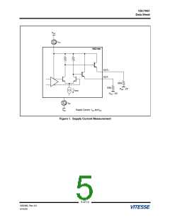
VSC7961
Data Sheet
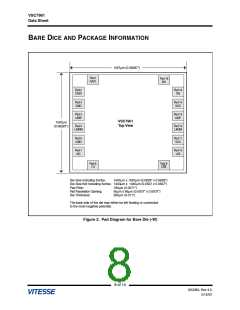
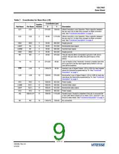
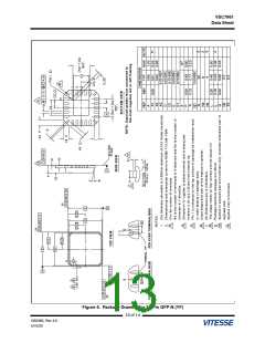
Table 7. Coordinates for Bare Dice (-W)
Coordinates (µm)
Pad/Pin
Number
Pad Name
Pin Name
X
Y
Description
CZ1
CZ1
1
270.525
1359.05
Offset Correction Loop Capacitor. Place capacitor between
this pin and CZ2 to alter time constant of offset correction
loop. See “Functional Description” on page 4.
CZ2
CZ2
2
80.95
1170.525 Offset Correction Loop Capacitor. Place capacitor between
this pin and CZ1 to alter time constant of offset correction
loop. See “Functional Description” on page 4.
GND
LAINP
LAINM
GND
GND
IN+
3
4
5
6
7
80.95
80.95
80.95
80.95
80.95
990.525
810.525
630.525
450.525
270.525
Supply ground.
Noninverted input signal.
Inverted input signal.
Supply ground.
IN–
GND
NC
NC
This pin may be either connected to ground or left uncon-
nected. This pin does not effect the performance of the
device.
TH
TH
8
9
270.525
1169.475
1359.05
80.95
80.95
Loss of Signal (LOS) Threshold. Connect a resistor from this
pin to ground to set the input signal level at which LOS out-
puts will be asserted.
LOS
LOS
LOS
LOS
Inverted Loss of Signal Output. LOS is HIGH for input signals
above the threshold programmed by TH. See “Functional
Description” on page 4.
10
270.525
Noninverted Loss of Signal Output. LOS is LOW for input sig-
nals above the threshold programmed by TH. See “Functional
Description” on page 4.
VCC
LOAM
LAOP
VCC
SQ
VCC
OUT–
11
12
13
14
15
1359.05
1359.05
1359.05
1359.05
1359.05
450.525
630.525
810.525
990.525
Power supply.
Inverted data output.
Noninverted data output.
Power supply.
OUT+
VCC
SQUELCH
1170.525 Squelch Input. Squelch is disabled if this pin is unconnected
or set LOW. When SQUELCH is HIGH, OUT+ and OUT– are
forced to static levels. See “Functional Description” on page 4.
NC
NC
16
1169.475
1359.05
No connection.
9 of 14
G52360, Rev 4.0
5/15/03

 VITESSE [ VITESSE SEMICONDUCTOR CORPORATION ]