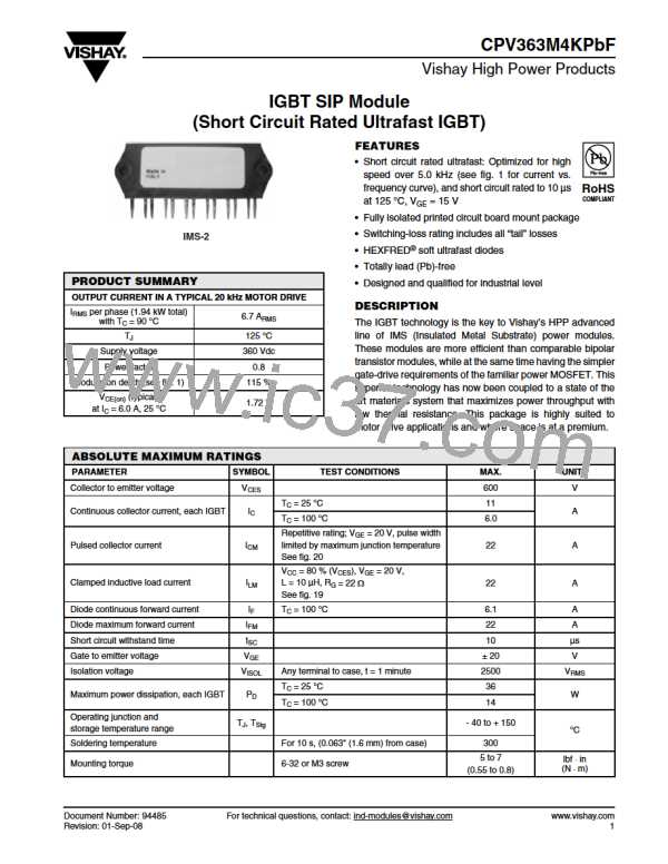
CPV363M4KPbF
IGBT SIP Module
(Short Circuit Rated
Ultrafast IGBT)
Vishay High Power Products
SWITCHING CHARACTERISTICS (TJ = 25 °C unless otherwise specified)
PARAMETER
SYMBOL
TEST CONDITIONS
MIN.
TYP.
61
MAX.
91
11
40
-
UNITS
Total gate charge (turn-on)
Gate to emitter charge (turn-on)
Gate to collector charge (turn-on)
Turn-on delay time
Rise time
Qg
-
-
-
-
-
-
-
-
-
-
IC = 6 A
Qge
Qgc
td(on)
tr
7.4
27
nC
VCC = 400 V
See fig. 8
55
24
-
TJ = 25 °C
I
V
ns
C = 6.0 A, VCC = 480 V
GE = 15 V, RG = 23 Ω
Energy losses include “tail” and diode
reverse recovery
Turn-off delay time
Fall time
td(off)
tf
107
92
160
140
-
Turn-on switching loss
Turn-off switching loss
Total switching loss
Eon
Eoff
Ets
0.28
0.10
0.39
See fig. 9, 10, 18
-
mJ
µs
0.50
VCC = 360 V, TJ = 125 °C
GE = 15 V, RG = 23 Ω, VCPK < 500 V
Short circuit withstand time
tSC
10
-
-
V
Turn-on delay time
Rise time
td(on)
tr
td(off)
tf
-
-
-
-
-
-
-
-
-
-
-
-
-
-
-
-
54
24
-
TJ = 150 °C
C = 6.0 A, VCC = 480 V
GE = 15 V, RG = 23 Ω
Energy losses include “tail” and
diode reverse recovery
See fig. 10, 11, 18
I
V
-
ns
Turn-off delay time
Fall time
161
244
0.60
740
100
9.3
42
-
-
-
Total switching loss
Input capacitance
Output capacitance
Reverse transfer capacitance
Ets
mJ
pF
Cies
Coes
Cres
-
VGE = 0 V
V
CC = 30 V
See fig. 7
-
ƒ = 1.0 MHz
-
TJ = 25 °C
TJ = 125 °C
TJ = 25 °C
TJ = 125 °C
TJ = 25 °C
TJ = 125 °C
TJ = 25 °C
TJ = 125 °C
60
120
6.0
10
180
600
-
Diode reverse recovery time
trr
See fig. 14
See fig. 15
See fig. 16
See fig. 17
ns
A
80
3.5
5.6
80
Diode peak reverse recovery current
Diode reverse recovery charge
Irr
IF = 12 A
R = 200 V
dI/dt = 200 A/µs
V
Qrr
nC
A/µs
220
180
120
Diode peak rate of fall of recovery
during tb
dI(rec)M/dt
-
Document Number: 94485
Revision: 01-Sep-08
For technical questions, contact: ind-modules@vishay.com
www.vishay.com
3

 VISHAY [ VISHAY ]