TMC8462 Datasheet • Document Revision V1.4 • 2018-May -09
190 / 204
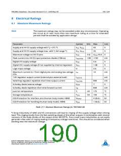
8 Electrical Ratings
8.1 Absolute Maximum Ratings
Note
The maximum ratings may not be exceeded under any circumstances. Operating
the circuit at or near more than one maximum rating at a time for extended
periods shall be avoided by application design.
Parameter
Symbol
VVS, VVIOx
VVS, VVIOx
VVIO
Min
Max
40
Unit
V
Supply and HV IO supply voltage with TJ = 0°C *)
Supply and HV IO supply voltage max. with TJ full range *)
Maximum voltage on HV IO pins
35
V
-0.6
VVIOx+0.6
V
Peak current into HV IO input protection diodes (100ms)
Digital I/O supply voltage
IHVIOPEAK
VVIO
-100 +100
mA
V
3.6
1.98
3.6
10
Digital VCC supply voltage (if not supplied by internal regulator)
Logic input voltage
VVCC
V
VI
V
Maximum current to / from digital pins and analog low voltage IIO
I/Os
mA
1.8V regulator output current (internal plus external load)
Switching regulator repetitive short time output current
Schottky diode reverse voltage
IVOUT18
mA
mA
V
IVOUTSW
VSDR
ISD
800
7
Schottky diode repetitive short time forward current
Junction temperature
800
mA
°C
TJ
-40
-55
175
Storage temperature
TSTG
VESDAP
VESD
150
°C
ESD-Protection for interface pins (Human body model, HBM)
ESD-Protection for handling (Human body model, HBM)
4 (tbd.)
1 (tbd.)
kV
kV
Table 211: Absolute Maximum Ratings for TMC8462-BA
*) Stray inductivity of GND and VS connections will lead to ringing of the supply voltage when driving
load. This ringing results from the fast switching slopes of the driver outputs in combination with reverse
recovery of the body diodes of the output driver MOSFETs. Even small trace inductivities as can easily
generate a few volts of ringing leading to temporary voltage overshoot. This should be considered when
working near the maximum voltage.
©2018 TRINAMIC Motion Control GmbH & Co. KG, Hamburg, Germany
Terms of delivery and rights to technical change reserved.
Download newest version at www.trinamic.com

 TRINAMIC [ TRINAMIC MOTION CONTROL GMBH & CO. KG. ]