TMC8462 Datasheet • Document Revision V1.4 • 2018-May -09
193 / 204
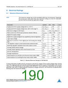
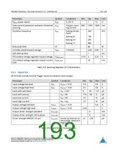
Parameter
Symbol
RON
Conditions
TJ=25 °C
Min Typ
1
Max
1.5
Unit
RDSon power switch
Ω
Over-current protection activation threshold IOCH
sourcing
Output sourc- 800 1200 1600 mA
ing current
Oscillator frequency
fOSC
Setting 00 (de-
fault)
240
kHz
Setting 01
Setting 10
Setting 11
130
470
890
83
Duty cycle limit
dl
%
Schottky diode forward voltage
Soft startup time
VSDF
I=350mA
0.60
1
0.80
5.25
V
ms
V
5V auxiliary voltage regulator output voltage VVDD5_OUT
4.75
5
5V auxiliary voltage regulator output current IVDD5_OUT
limit
10
mV
Table 214: Switching Regulator DC Characteristics
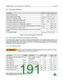
8.3.3 Digital IOs
All I/O lines include Schmitt-Trigger inputs to enhance noise margin.
Parameter
Symbol Conditions
Min
-0.3
2.3
5
Typ
30
Max Unit
Input voltage low level
Input voltage high level
Input with pull-down
VINL
VINH
VVCCIO = 3.3V
VVCCIO = 3.3V
VIN = 3.3V
VIN = 0V
0.8
3.6
110
-5
V
V
µA
µA
µA
µA
V
Input with pull-up
-110 -30
-10
Input low current
VIN = 0V
10
Input high current
VIN = VDD
-10
10
Output voltage low level
Output voltage high level
Output driver strength standard
Output driver strength LED outputs
Driver strength NRESET I/O pin
VOUTL
VVCCIO = 3.3V
VVCCIO = 3.3V
0.4
VOUTH
2.64
4
V
IOUT_DRV
IOUT_LED
mA
mA
µA
8
IOUT_RST Driven by internal un- ±5
dervoltage detectors
High/Low
±30
Table 215: Digital IOs DC Characteristics
©2018 TRINAMIC Motion Control GmbH & Co. KG, Hamburg, Germany
Terms of delivery and rights to technical change reserved.
Download newest version at www.trinamic.com

 TRINAMIC [ TRINAMIC MOTION CONTROL GMBH & CO. KG. ]