TMC8462 Datasheet • Document Revision V1.4 • 2018-May -09
191 / 204
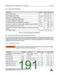
8.2 Operational Ratings
Parameter
Symbol
TJ
Min Max Unit
Junction temperature
-40
125
°C
V
High voltage supply voltage
VVS,VS0,VS1 4.75 34
VVCCIO 3.15 3.45
VVIOx
Digital I/O 3.3V supply voltage
I/O supply voltage (high voltage mode)
I/O Supply voltage (low voltage mode)
Continuous output current single high voltage I/O
V
6.0
3.0
34
V
VVIOx
5.5
100
200
500
5.5
V
IOUT,HVIO
mA
mA
mA
V
Continuous current into / from any high voltage I/O supply or GND pin IIN,HVIO
Switching regulator DC output current
IOUT,SW
3.3V Switching regulator supply voltage when using internal Schottky
diode
4
Core supply voltage
VVCC_CORE 1.65 1.95
V
Table 212: Operational Ratings for TMC8462-BA
8.3 DC Characteristics and Timing Characteristics
DC characteristics contain the spread of values guaranteed within the specified supply voltage range
unless otherwise specified. Typical values represent the average value of all parts measured at +25 C.
°
Temperature variation also causes stray to some values. A device with typical values will not leave Min/Max
range within the full temperature range.
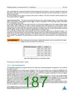
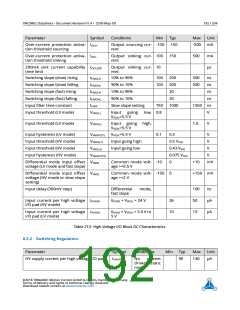
8.3.1 High Voltage I/O Block
When driving inductive loads a freewheeling diode must be provided to the high
voltage I/O pins to prevent from latch-up.
WARNING
Parameter
Symbol
Conditions
Min
Typ
90
Max
140
Unit
µA
HV supply current per high volt- IVHVIO
age I/O pad
No current driven,
static mode
RDSon low side
RONL
RONH
RONH
IPD
TJ=25 °C
6
10
Ω
RDSon high side
VVIOx=5 V; TJ=25 °C
VVIOx=3.3 V; TJ=25 °C
10
13
63
110
76
15
Ω
RDSon high side
20
Ω
Weak pull down current
Weak pull up current
Weak pull up current
37
66
50
115
210
150
µA
µA
µA
IPU
VVIOx=5 V; TJ=25 °C
VVIOx=3.3 V; TJ=25 °C
IPU
©2018 TRINAMIC Motion Control GmbH & Co. KG, Hamburg, Germany
Terms of delivery and rights to technical change reserved.
Download newest version at www.trinamic.com

 TRINAMIC [ TRINAMIC MOTION CONTROL GMBH & CO. KG. ]