TMC8462 Datasheet • Document Revision V1.4 • 2018-May -09
188 / 204
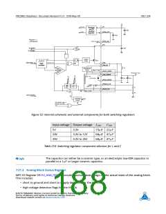
+VS
Undervolt
VS
Bandgap
and 5V
100nF
auxiliary
regulator
1.2V Ref
VDD5_OUT
470nF
Regulator 1 /
Switch reg supply
3.3V Regulator
VDD5_INx
VSx
SC_DETECT
100nF
IMAX
SC_DISABLE
Set
PMOS
Driver
1
S
R
Q
MOSFET
Dutycycle limit
SAW_FREQ[1..0]
SWx
SAW
SWx_IN
oscillator
+
+
-
LSW
Dampening
Circuit
Sum
Amplifier
Compa-
rator
&
Reg. 1 only
VOUT1_DAMP
SW0_DIODE
SW regulator output
+VIO
0.8A Schottky
CSW
CSWE
GND0_DIODE
VREG3V3_FB
53k
92k
RFB
CFB
RV1
VOUT1_FB
Reg. 1 only
250k
RV2
VOUT_DISABLE
0→
1.2V
1.2V Ref
Soft Start
Circuit
VOUT_DISABLE (Reg. 1)
Overtemp (3.3V Reg.)
/
Disable
UV
Figure 52: Internal schematic and external components for both switching regulators
Input voltage Output voltage LSW
CSW
5V
3.3V
15µH 22µF
68µH 47µF
68µH 47µF
24V
35V
3.3V to 12V
3.3V to 25V
Table 210: Switching regulator component selection for L and C
The capacitor can either be a ceramic type, or an electrolytic low-ESR capacitor in
parallel to a 1µF or larger ceramic capacitor.
Info
7.21.3 Analog Block Status Register
MFC IO Register 59 HV_ANA_STATUS provides various status flags on the actual state of the analog block.
This includes:
• short to ground and short to supply detection for the HV IOs
• high voltage detection flags for the HV IOs
©2018 TRINAMIC Motion Control GmbH & Co. KG, Hamburg, Germany
Terms of delivery and rights to technical change reserved.
Download newest version at www.trinamic.com

 TRINAMIC [ TRINAMIC MOTION CONTROL GMBH & CO. KG. ]