TMC6200 DATASHEET (Rev. 1.01 / 2018-NOV-15)
8
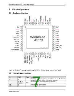
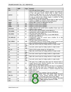
Pin
LSU
TQFP
5
Type Function
Low side gate driver output.
Output of internal 11.5V gate voltage regulator and supply pin
of low side gate drivers. Attach 2.2µF to 22µF ceramic
capacitor to GND plane near to pin for best performance. Use
at least 5-10 times more capacity than for bootstrap capacitors.
In case an external gate voltage supply is available, tie VSA
and 12VOUT to the external supply.
Output of internal 5V regulator. Attach 2.2µF to 10µF ceramic
capacitor to GNDA near to pin for best performance.
Analog GND. Connect to GND plane near pin.
Output of current sense amplifier.
12VOUT
6
7
5VOUT
GNDA
CURU
CURV
CURW
8
9
10
11
AO
AO
AO
Output of current sense amplifier.
Output of current sense amplifier.
Center reference for current sense amplifiers (leave open for
5VOUT/3 offset voltage).
SPI chip select input (negative active) (SPE=1) or
Configuration input for gate driver current LSB (SPE=0)
SPI serial clock input (SPE=1) or
VOFS/TEST
CSN_IDRV0
SCK_IDRV1
12
13
14
AI
DI
DI
Configuration input for gate driver current MSB (SPE=0)
SPI data input (SPE=1) or
Configuration input for current sense amplifier 5x or 10x
amplification (SPE=0)
SDI_AMPLx10
15
DI
SPI data output (tristate) (SPE=1) or
SDO_SINGLE
UH
16
17
DIO
Configuration input for internal bridge control mode (0: dual
line, 1: xH=phase polarity, xL=phase enable) (SPE=0)
High side control input (or bridge polarity in single mode)
DI
(pd)
DI
(pd)
Low side control input (or bridge enable in single mode)
UL
18
19
20
VCC_IO
VH
3.3V to 5V IO supply voltage for all digital pins.
High side control input (or bridge polarity in single mode)
DI
(pd)
DI
(pd)
DI
(pd)
DI
Low side control input (or bridge enable in single mode)
High side control input (or bridge polarity in single mode)
Low side control input (or bridge enable in single mode)
VL
21
22
23
WH
WL
(pd)
CLK input. Tie to GND using short wire for internal clock or
supply external clock. Internal clock-fail over circuit protects
against loss of external clock signal.
Mode selection input. When tied low, the chip is in standalone
mode and SPI pins have their configuration pin functions.
When tied high, the SPI interface is enabled. Integrated pull
down resistor.
CLK
SPE
24
25
DI
DI
(pd)
Diagnostics output.
FAULT
26
27
DO
DI
High upon driver error condition. Clear by cycling EN.
Positive active enable input. The power stage becomes
switched off (all motor outputs floating) when this pin
becomes driven to a low level. Cycle low to clear FAULT.
Analog supply voltage for 11.5V and 5V regulator. Normally
tied to VS. Provide a 100nF filtering capacitor to GND.
Charge pump capacitor output.
DRV_EN
VSA
CPO
29
30
www.trinamic.com

 TRINAMIC [ TRINAMIC MOTION CONTROL GMBH & CO. KG. ]