TMC6200 DATASHEET (Rev. 1.01 / 2018-NOV-15)
23
GENERAL CONFIGURATION REGISTERS (0X00…0X0F)
R/W
Addr
n
Register
Description / bit names
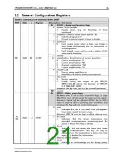
11 OT150°C
31.. VERSION: 0x10=first version of the IC
24 Identical numbers mean full digital compatibility.
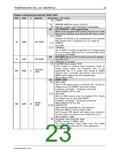
Bit
OTP_PROGRAM – OTP programming
Write access programs OTP memory (one bit at a time),
Read access refreshes read data from OTP after a write
2..0 OTPBIT
Selection of OTP bit to be programmed to the selected
byte location (n=0..7: programs bit n to a logic 1)
5..4 OTPBYTE
Set to 00
15..8 OTPMAGIC
Set to 0xbd to enable programming. A programming
W
0x06
OTP_PROG
OTP_READ
time of minimum 10ms per bit is recommended (check
by reading OTP_READ).
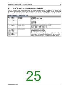
OTP_READ (Access to OTP memory result and update)
See table 5.1.1!
Bit
R
0x07
0x08
7..0 OTP0 byte 0 read data
4..0 FCLKTRIM (Reset default: OTP)
0…31: Lowest to highest clock frequency. Check at
charge pump output. The frequency span is not
guaranteed, but it is tested, that tuning to 12MHz
internal clock is possible. The devices come preset to
12MHz clock frequency by OTP programming.
(Reset Default: OTP)
FACTORY_
CONF
RW
5
Bit
SHORT_CONF
3..0 S2VS_LEVEL:
Short to VS detector level for lowside FETs. Checks for
voltage drop in LS MOSFET and sense resistor.
1 (highest sensitivity) … 15 (lowest sensitivity)
(Reset Default: OTP 6 or 12)
11..8 S2G_LEVEL:
Short to GND detector level for highside FETs. Checks
for voltage drop on high side MOSFET
2 (highest sensitivity) … 15 (lowest sensitivity)
(Reset Default: OTP 6 or 12)
SHORT_
CONF
RW
0x09
19
17..16 SHORTFILTER:
Spike filtering bandwidth for short detection
0 (lowest, 100ns), 1 (1µs), 2 (2µs) 3 (3µs)
Hint: A good PCB layout will allow using setting 0.
Increase value, if erroneous short detection occurs.
(Reset Default = %01)
20 shortdelay: Short detection delay
0=750ns: normal, 1=1500ns: high
The short detection delay shall cover the bridge
switching time. 0 will work for most applications.
(Reset Default = 0)
www.trinamic.com

 TRINAMIC [ TRINAMIC MOTION CONTROL GMBH & CO. KG. ]