TMC248-LA DATASHEET (Rev. 1.01 / 2013-MAR-26)
6
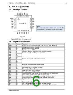
2 Pin Assignments
2.1 Package Outline
28 27 26 25 24 23 22
AGND
ANN
HA1
HA2
LA1
BL2
HB1
HB2
LB1
LB2
SRB
BL1
TMC248-LA
LA2
SRA
Note:
The exposed die attach pad should be
connected to a GND plane or can be left open.
8
9
10 11 12 13 14
Top view
Figure 2.1 TMC248 pin assignments
2.2 Signal Descriptions
Pin
Number Function
AGND
INA
INB
GND
OSC
HA1
HA2
HB1
HB2
LA1
LA2
LB1
LB2
SRA
SRB
SDO
SDI
SCK
CSN
SPE
SLP
ENN
ANN
BL1
BL2
VS
1
Analog ground (reference for SRA, SRB, OSC, SLP, INA, INB, SLP)
Analog current control phase A
Analog current control phase B
Digital and power GND
Oscillator capacitor or external clock input for chopper
27
26
24
8
3
4
20
19
5
Outputs for high side P-channel transistors.
Outputs for low side N-channel transistors
Bridge A / B current sense resistor input
6
18
17
7
16
9
10
11
12
14
28
13
2
15
21
23
25
22
Data output of SPI interface (tri-state)
Data input of SPI interface
Serial clock input of SPI interface
Chip select input of SPI interface
Enable SPI mode (high active). Tie to GND for non-SPI applications
Slope control resistor. Tie to GND for fastest slope
Device enable (low active) and overvoltage shutdown input
Enable analog current control via INA and INB (low active)
Digital blank time select
Motor supply voltage
3.0… 5.5V supply voltage for analog and logic circuits
Short to GND detection comparator – connect to VS if not used
VCC
VT
www.trinamic.com

 TRINAMIC [ TRINAMIC MOTION CONTROL GMBH & CO. KG. ]