TMC248-LA DATASHEET (Rev. 1.01 / 2013-MAR-26)
10
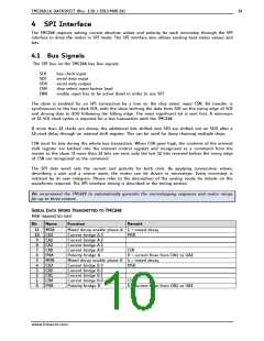
4 SPI Interface
The TMC248 requires setting current absolute values and polarity for each microstep through the SPI
interface to drive the motor in SPI mode. The SPI interface also allows reading back status values and
bits.
4.1 Bus Signals
The SPI bus on the TMC248 has five signals:
SCK
SDI
SDO
CSN
ENN
bus clock input
serial data input
serial data output
chip select input (active low)
enable input has to be active (low) in order to use SPI
The slave is enabled for an SPI transaction by a low on the chip select input CSN. Bit transfer is
synchronous to the bus clock SCK, with the slave latching the data from SDI on the rising edge of SCK
and driving data to SDO following the falling edge. The most significant bit is sent first. A minimum
of 12 SCK clock cycles is required for a bus transaction with the TMC248.
If more than 12 clocks are driven, the additional bits shifted into SDI are shifted out on SDO after a
12-clock delay through an internal shift register. This can be used for daisy chaining multiple chips.
CSN must be low during the whole bus transaction. When CSN goes high, the contents of the internal
shift register are latched into the internal control register and recognized as a command from the
master to the slave. If more than 12 bits are sent, only the last 12 bits received before the rising edge
of CSN are recognized as the command.
The SPI data word sets the current and polarity for both coils. By applying consecutive values,
describing a sine and a cosine wave, the motor can be driven in microsteps. Every microstep is
initiated by its own telegram. Please refer to the description of the analog mode for details on the
waveforms required. The SPI interface timing is described in the timing section.
We recommend the TMC429 to automatically generate the microstepping sequence and motor ramps
for up to three motors.
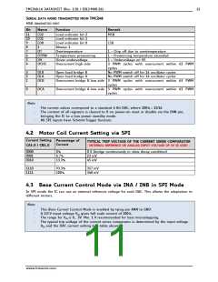
SERIAL DATA WORD TRANSMITTED TO TMC248
MSB TRANSMITTED FIRST
Bit
Name
Function
Remark
11 MDA
10 CA3
Mixed decay enable phase A 1 = mixed decay
Current bridge A.3
Current bridge A.2
Current bridge A.1
Current bridge A.0
Polarity bridge A
MSB
9
8
7
6
5
4
3
2
1
0
CA2
CA1
CA0
PHA
MDB
CB3
CB2
CB1
CB0
PHB
LSB
0 = current flow from OA1 to OA2
Mixed decay enable phase B 1 = mixed decay
Current bridge B.3
Current bridge B.2
Current bridge B.1
Current bridge B.0
Polarity bridge B
MSB
LSB
0 = current flow from OB1 to OB2
www.trinamic.com

 TRINAMIC [ TRINAMIC MOTION CONTROL GMBH & CO. KG. ]