TMC248-LA DATASHEET (Rev. 1.01 / 2013-MAR-26)
28
11 MOSFET Examples
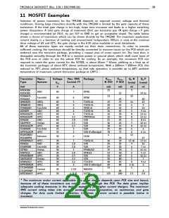
Selection of power transistors for the TMC248 depends on required current, voltage and thermal
conditions. Driving large transistors directly with the TMC248 is limited by the gate capacity of these
transistors. If the total gate charge is too high, slope time increases and leads to a higher switching
power dissipation. A total gate charge of maximum 25nC per transistor pair (N gate charge + P gate
charge) is recommended (at 25nC, tie pin SLP to GND to get an acceptable slope). The table below
shows a choice of transistors which can be driven directly by the TMC248. The maximum application
current mainly is a function of cooling and environment temperature. RDSon is read at the nominal
drive voltage of 6V and 25°C, the gate charge is the 4.5V value available in most datasheets.
All of these transistor types are mainly cooled via their drain connections. In order to provide
sufficient cooling, the transistors should be directly connected to massive traces on the PCB which are
widened near the transistor package, providing a copper area of some square cm. The heat then is
dissipated vertically through the PCB to a massive power or ground plane, which shall cover most of
the PCB area in order to use the whole PCB for cooling. As an example, the minimum PCB size
required to reach the given current for the SI7501, is about 42mm * 42mm, yielding in a heat up of
the transistor packages of about 85°C above ambient temperature. With a 100mm * 100mm PCB, this
reduced to 70°C above ambient temperature, so that safe operation is possible up to 60°C ambient
temperature at maximum current (transistor package at 130°C).
Transistor Manu-
Voltage
Max. RMS Package
Current (*)
RDSon
N (5V) P (6V)
RDSon
QG N
(note) (note)
QG P
Type
facturer
VDS
V
Unit
A
mΩ
mΩ
nC
nC
AOD4186
AOD4185
15
9
A&O
40
40
7
6
DPAK..
DPAK
15
19 (1)
FDD8647L
FDD4243
QM4302D
QM4803D
FDD8424H
AOD609
AP4543GEH
AP4543GMT
AO4618
SI4599DY
AP4543GEM
FDS8960C
AP9934AGM
BSZ050N03
BSZ180P03
AP4509AGH
AO4616
FDS8958B
SI7501
AON7611
AP4503BGM
SI4532ADY
AP2852GO
AP9930AGM
CTLDM303N
CTLDM304P
AP2530AGY
13
12
Fairchild
45
35
45
45
45
50
50
22
45
55
60
75
18
12
9
UBIQ
UBIQ
Fairchild
A&O
APEC
APEC
A&O
Vishay
APEC
Fairchild
APEC
40
40
40
40
40
40
40
40
40
35
35
5
4
4
4
4
3.5
2.8
2.5
2.5
3
TO252-4L
TO252-4L
DPAK-4L
TO252-4L
TO252-4L
PMPAK5x6
SO8
SO8
SO8
SO8
15
28
25
31
32
32
21
36
38
25
70
6
11
6
9
5
8
8
3
5
8
14
9 (1)
13 (1)
13 (1)
8 (1)
12 (1)
12 (1)
6
6
6
13
2
SO8 (Fullbridge)
6 (1)
Infineon
30
6
S3O8
18
32
25
50
50
40
40
80
65
80
15
17 (1)
16
7 (1)
11 (1)
5 (1)
12 (1)
7
APEC
A&O
Fairchild
Vishay
A&O
APEC
Vishay
APEC
30
30
30
30
30
30
30
30
30
7
TO252-4L
SO8
SO8
PPAK1212
DFN3x3
SO8
16
24
29
35
53
35
50
48
60
33
15 (2)
9
4
5
2
6
5
8
6 (2)
5
2.8
2.8
3
2.8
2.5
2.3
2.2
2
SO8
TSSOP-8
SO8 (Fullbridge)
9 (1)
6
APEC
Central
APEC
30
30
2 (3)
M832DS
SOT26
64
200
6
2.8
1 (1.5)
135
2.5
* The maximum motor current applicable in a given design depends upon PCB size and layout,
because all of these transistors are mainly cooled through the PCB. The data given implies
adequate cooling measures in the design, especially for higher current designs. The maximum
RMS current rating takes into account package power dissipation, on resistances, and gate
charges. For duty cycle limited operation, 1.5 times or more current is possible (value in
brackets).
www.trinamic.com

 TRINAMIC [ TRINAMIC MOTION CONTROL GMBH & CO. KG. ]