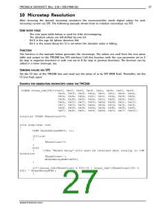
TMC248-LA DATASHEET (Rev. 1.01 / 2013-MAR-26)
31
12.3 Pull-up Resistors on Unused Inputs
The digital inputs all have integrated pull-up resistors, except for the ENN input, which is in fact an
analog input. Thus, there are no external pull-up resistors required for unused digital inputs which are
meant to be positive.
12.4 Power Supply Sequencing Considerations
Upon power up, the driver initializes and switches off the bridge power transistors. The Vcc supply
voltage has to be at least 1.0 V and the Vs supply voltage has to be at least 5.0 V. This is a pre-
condition for the internal startup logic to work properly.
When Vs goes up with Vcc at 0 V, a medium current temporary cross conduction of the power stage
can result at supply voltages between 2.4 V and 4.8 V. In this voltage range, the upper transistors
conduct, while the gates of the lower transistors are floating. While this typically does no harm to the
driver, it may hinder the power supply from coming up properly, depending on the power supply
start up behavior.
THERE ARE TWO POSSIBILITIES TO PREVENT THIS:
-
Add resistors from the LA and LB outputs to GND in the range of 1M keeping the low side
N-channel MOSFETs gates at GND.
-
Alternatively, either use a dual voltage power supply, or use a local regulator, generating the
5 V or 3.3 V Vcc voltages.
Attention
Some switching regulators do not start before the input voltage has reached 5V. Therefore it is
recommended to use a standard linear regulator like 7805 or LM317 series or a low drop regulator or
a switching regulator like the LM2595, starting at relatively low input voltages.
www.trinamic.com

 TRINAMIC [ TRINAMIC MOTION CONTROL GMBH & CO. KG. ]