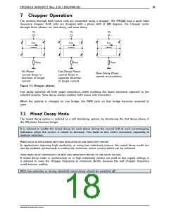
TMC248-LA DATASHEET (Rev. 1.01 / 2013-MAR-26)
14
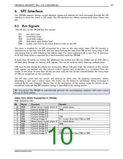
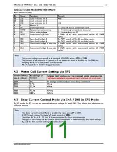
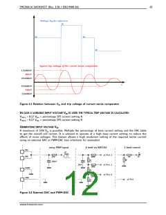
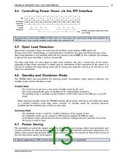
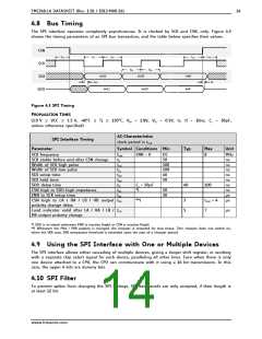
4.8 Bus Timing
The SPI interface operates completely asynchronous. It is clocked by SCK and CSN, only. Figure 4.3
shows the timing parameters of an SPI bus transaction, and the table below specifies their values.
CSN
tCC
tCL
tCH
tCH
tCC
SCK
SDI
tDU
tDH
bit11
bit10
bit0
bit0
tDO
tZC
bit11
bit10
SDO
Figure 4.3 SPI Timing
PROPAGATION TIMES
(3.0 V VCC 5.5 V, -40°C Tj 150°C; VIH = 2.8V, VIL = 0.5V; tr, tf = 10ns; CL = 50pF,
unless otherwise specified)
AC-Characteristics
SPI Interface Timing
clock period is tCLK
Parameter
Symbol Conditions Min
Typ
Max
Unit
SCK frequency
fSCK
t1
ENN = 0
DC
50
100
100
40
8
MHz
ns
ns
ns
ns
ns
ns
ns
µs
µs
SCK stable before and after CSN change
Width of SCK high pulse
Width of SCK low pulse
SDI setup time
SDI hold time
SDO delay time
CSN high to SDO high impedance
ENN to SCK setup time
CSN high to LA / HA / LB / HB output tPD
polarity change delay
Load indicator valid after LA / HA / LB / tLD
HB output polarity change
tCH
tCL
tDU
tDH
tD
50
CL = 50pF
*)
40
100
tZC
tES
50
30
**)
3
5
tOSC + 4
7
µs
*) SDO is tri-stated whenever ENN is inactive (high) or CSN is inactive (high).
**) Whenever the PHA / PHB polarity is changed, the chopper is restarted for that phase. Tthe chopper does not switch on,
when the SRA resp. SRB comparator threshold is exceeded upon the start of a chopper period.
4.9 Using the SPI Interface with One or Multiple Devices
The SPI interface allows either cascading of multiple devices, giving a longer shift register, or working
with a separate chip select signal for each device, paralleling all other lines. Even when there is only
one device attached to a CPU, the CPU can communicate with it using a 16 bit transmission. In this
case, the upper 4 bits are dummy bits.
4.10 SPI Filter
To prevent spikes from changing the SPI settings, SPI data words are only accepted, if their length is
at least 12 bit.
www.trinamic.com

 TRINAMIC [ TRINAMIC MOTION CONTROL GMBH & CO. KG. ]