XC9128/XC9129
Series
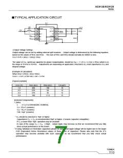
■TYPICAL APPLICATION CIRCUIT
<Output Voltage Setting>
Output voltage can be set by adding external split resistors. Output voltage is determined by the following equation,
based on the values of RFB1 and RFB2. The sum of RFB1 and RFB2 should normally be 500kΩ or less.
VOUT=0.45 × (RFB1 + RFB2) / RFB2
The value of CFB, speed-up capacitor for phase compensation, should be fZFB = 1 / (2 x π x CFB1 x RFB1) which is in
the range of 10 kHz to 50 kHz. Adjustments are depending on application, inductance (L), load capacitance (CL) and
dropout voltage.
[Example of calculation]
When RFB1=270kΩ, RFB2=43kΩ,
VOUT1 = 0.45 × (270k+43k ) / 43k = 3.276V
[Typical example]
RFB1 (kΩ)
300
RFB2 (kΩ)
100
VOUT (V)
1.8
CFB (pF)
10
2.5
270
59
12
3.3
270
43
12
5.0
180
17.8
15
[External Components]
1.2MHz:
L
: 4.7μH (CDRH4D28C SUMIDA)
CL1: 22μF (ceramic)
CL2: 10μF (ceramic)
CIN: 10μF (ceramic)
* CL1 should be selected in 10μF or higher.
Capacitance CL1 + CL2 is recommended 30μF or higher. (Ceramic capacitor compatible)
If CL1 is lower than 10μF, operation may be unstable.
In case of the usage CL1 + CL2 <30μF, output ripple may increase so that we recommend that you fully
check actual performance on the board.
* If using Tantalum or Electrolytic capacitors please be aware that ripple voltage will be higher due to the larger
ESR (Equivalent Series Resistance) values of those types of capacitors. Please also note that the IC’s
operation may become unstable with such capacitors so we recommend that you fully check actual
performance.
7/13

 TOREX [ Torex Semiconductor ]