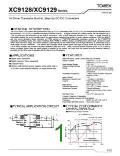
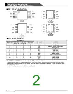
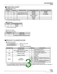
XC9128/XC9129 Series
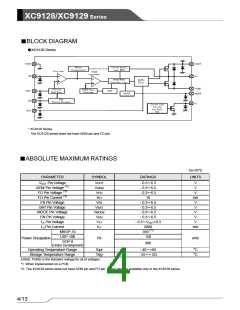
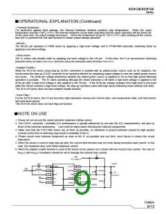
■BLOCK DIAGRAM
●XC9128 Series
* XC9129 Series
The XC9129 series does not have AEN/ pin and FO pin.
■ABSOLUTE MAXIMUM RATINGS
Ta=25℃
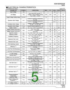
PARAMETER
SYMBOL
RATINGS
UNITS
VOUT Pin Voltage
AEN/ Pin Voltage (*2)
FO Pin Voltage (*2)
FO Pin Current (*2)
FB Pin Voltage
VOUT
VAEN/
VFO
- 0.3~6.5
- 0.3~6.5
- 0.3~6.5
10
V
V
V
IFO
mA
V
VFB
- 0.3~6.5
- 0.3~6.5
- 0.3~6.5
- 0.3~6.5
- 0.3~VOUT+0.3
2000
BAT Pin Voltage
MODE Pin Voltage
EN Pin Voltage
VBAT
VMODE
VEN
V
V
V
LX Pin Voltage
VLx
V
LX Pin Current
ILx
mA
MSOP-10
350 (*1)
USP-10B
150
Power Dissipation
Pd
mW
SOP-8
(Under Development)
Operating Temperature Range
Storage Temperature Range
300
Topr
Tstg
- 40~+85
oC
oC
- 55~+125
AGND, PGND is the standard voltage for all of voltages.
*1: When implemented on a PCB.
*2: The XC9129 series does not have AEN/ pin and FO pin. These pins are available only in the XC9128 series.
4/13

 TOREX [ Torex Semiconductor ]