XC9128/XC9129 Series
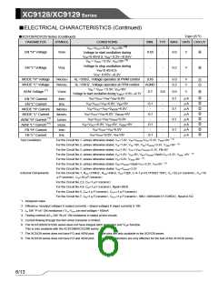
■ELECTRICAL CHARACTERISTICS (Continued)
Topr=25 oC
●XC9128/XC9129 Series (Continued)
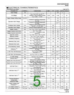
PARAMETER
EN "H" Voltage
SYMBOL
VENH
CONDITIONS
MIN.
0.65
TYP. MAX. UNITS CIRCUIT
VIN =VOUT=3.3V, VFO=0V (*8)
Voltage to start oscillation during
VFB=0.45×0.9, VEN= 0.2V→0.65V
VIN = VOUT =3.3V, VFO=0V (*8)
-
-
6.0
0.2
V
V
④
④
Voltage to stop oscillation during
VFB=0.45×0.9,
EN "L" Voltage
VENL
-
VEN= 0.65V→0.2V
MODE "H" Voltage
MODE "L" Voltage
VMODEH
VMODEL
RL =330Ω, Voltage operates at PWM control
RL =330Ω, Voltage operates at PFM control
VIN = VOUT =3.3V, VFO=0V
0.65
-
-
6.0
0.2
V
V
①
①
AGND
AEN/ Voltage (*7)
VAEN/
0.7
0.8
0.9
V
④
Voltage to start oscillation during VAEN/= 0.9V
→0.7V
②
②
②
②
②
②
②
②
VIN=VOUT=VFB=VEN=6.0V
-
-0.1
-
-
-
-
-
-
-
-
-
0.1
-
μA
μA
μA
μA
μA
μA
μA
μA
EN "H" Current
EN "L" Current
IENH
IENL
VIN=VOUT=VFB=6.0V, VEN=0V
VIN=VOUT=VFB=VMODE=6.0V
VIN=VOUT=VFB=6.0V, VMODE=0V
VIN=VOUT=VFB=VAEN/=6.0V
0.1
-
MODE "H" Current
MODE "L" Current
AEN/ "H" Current (*7)
AEN/ "L" Current (*7)
FB "H" Current
IMODEH
IMODEL
IAEN/H
IAEN/L
IFBH
-0.1
-
0.1
-
VIN=VOUT=6.0V, VEN=0V, VAEN/=0V
VIN=VOUT=VFB=6.0V
-0.1
-
0.1
-
VIN=VOUT=6.0V, VFB=0V
-0.1
FB "L" Current
IFBL
*8
)
(
Test Conditions:
For the Circuit No.1, unless otherwise stated, VIN=1.8V, VEN=VMODE=VFO=3.3V, VAEN/=0V
*8
)
(
For the Circuit No.2, unless otherwise stated, VIN=1.8V, VFB =0V, VEN=VMODE=3.3V, VAEN/=0V
For the Circuit No.3, unless otherwise stated, VIN=1.8V, VOUT=VEN=VMODE=3.3V, FB=0V
*8
)
(
For the Circuit No.4, unless otherwise stated, VIN=1.8V, VFB=0V, VEN=VMODE=Vpull=VFO=3.3V, VAEN/ =0V
*8
)
(
For the Circuit No.5, unless otherwise stated, VIN=3.3V, VAEN/=0V
*8
)
(
For the Circuit No.6, unless otherwise stated, VEN=VMODE=Vpull=VFO=3.3V, VFB=0V
For the Circuit No.7, unless otherwise stated, VEN=VMODE=3.3V
External Components:
For the Circuit No.1, RFB1=270kΩ, RFB2=43kΩ, CFB=12pF, L=4.7μH(LTF5022 TDK), CL1=22μF(ceramic), CL2=10
μF(ceramic), CIN=10μF(ceramic)
For the Circuit No.2,3, CIN=1μF(ceramic)
For the Circuit No.4,6, CIN=1μF(ceramic), Rpull=300Ω
For the Circuit No.5, CIN=1μF(ceramic), COUT=1μF(ceramic)
For the Circuit No.7, CIN=1μF(ceramic), COUT=1μF(ceramic), SBD =XBS304S17(TOREX), Rpull=0.5Ω
*1 : Designed value
*2 : Efficiency ={(output voltage) X (output current)} ÷ {(input voltage) X (input current)} X 100
*3 : LX SW "P-ch" ON resistance=(VLx-VOUT pin test voltage)÷100mA
*4 : Testing method of LX SW "N-ch" ON resistance is stated at test circuits.
*5 : Current flowing through the Nch driver transistor is limited.
*6 : The XC9128D/XC9129D series does not have integral latch protection and VLVP function.
This is only available with the XC9128B/XC9129B series.
*7 : The XC9129 series does not have FO and AEN/ pins. These pins are only available in the XC9128 series.
*8 : The XC9129 series does not have FO and AEN/ pins. The AEN/FO functions are only effective for the test of the XC9128 series.
6/13

 TOREX [ Torex Semiconductor ]