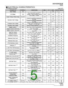
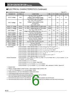
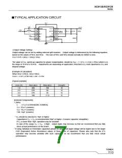
XC9128/XC9129
Series
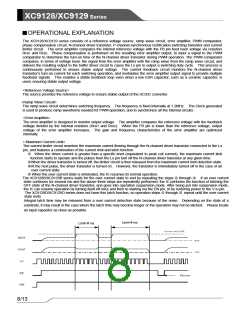
■TEST CIRCUITS *1
< Circuit No.1 >
Wave Form Measure Point
L
Lx
VOUT
MODE
FB
CFB
A
BAT
RFB1
A
※
External Components
4.7uH(LTF5022T-4R7N2R0 : TDK)
CIN : 10uF (ceramic)
CL1 : 22uF (ceramic)
CL2 : 10uF (ceramic)
CL1
EN
V
CIN
RL
VIN
V
L
:
CL2
VMODE
VEN
10kΩ
V
FO
AEN/
AGND
RFB2
VAEN/
VFO
PGND
Wave Form Measure Point
< Circuit No.2 >
< Circuit No.3 >
Lx
Lx
VOUT
VOUT
MODE
FB
A
BAT
EN
A
A
BAT
EN
MODE
FB
A
A
VMODE
VOUT
CIN
CIN
VIN
FB
VIN
VMODE
FO
AEN/
AGND
FO
AEN/
VFB
A
VEN
VAEN/
VEN
PGND
PGND
AGND
CIN : 1uF (ceramic)
※
External Components
※ External Components
CIN : 1uF (ceramic)
< Circuit No.4 >
<Circuit No.5 >
Wave Form Measure Point
Rpull
Lx
VOUT
MODE
FB
Lx
VOUT
MODE
FB
Vpull
BAT
EN
A
BAT
EN
A
VMODE
VOUT
COUT
VIN
CIN
CIN
VLx
FB
VFB
VEN
VAEN/
A
VFO
FO
AEN/
FO
AEN/
AGND
VIN
VAEN/
PGND
AGND
PGND
※
External Components
※
External Components
CIN
: 1uF (ceramic)
CIN : 1uF (ceramic)
COUT : 1uF (ceramic)
Rpull : 300Ω
<Circuit No.7 >
<Circuit No.6 >
Wave Form Measure Point
Rpull
Wave Form Measure Point
Lx
VOUT
Lx
VOUT
V1
Rpull
SBD
Vpull
A
BAT
EN
MODE
FB
BAT
EN
MODE
FB
Vpull
VOUT
VIN
CLX
CIN
CIN
V
COUT
VEN
VMODE
VOUT
VIN
A
VFO
FO
AEN/
AGND
FO
AEN/
AGND
FB
VEN
VMODE
PGND
PGND
※
External Components
CIN
: 1uF (ceramic)
※
External Components
CIN : 1uF (ceramic)
COUT : 1uF (ceramic)
SBD : XBS304S17(TOREX)
Rpull 0.5Ω
Rpull : 300Ω
:
Measurement method for ON resistance of the Lx switch
Using the layout of circuit No.7 above, set the LX pin voltage to 50mV by adjusting the Vpull voltage whilst the N-ch driver
transistor is turned on. Then, measure the voltage difference between both ends of Rpull. ON Resistance is calculated by using
the following formula:
R
LXN=0.05 ÷ ((V1 – 0.05) ÷ 0.5)
where V1 is a voltage between SBD and Rpull. LX pin voltage and V1 are measured by an oscilloscope.
*1: The XC9129 series does not have the AEN/ pin and the FO pin. When the XC9129 series is measured, the FO and AEN
pins are not effective in the above mentioned test circuits, they are NC.
11/13

 TOREX [ Torex Semiconductor ]