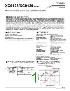
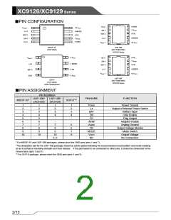
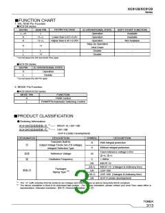
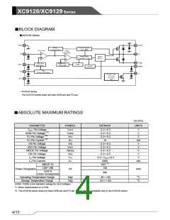
XC9128/XC9129
Series
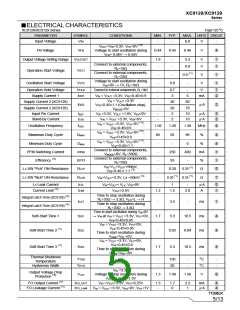
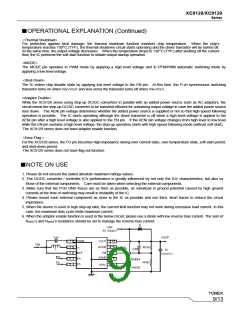
■ELECTRICAL CHARACTERISTICS
XC9128/XC9129 Series
Topr=25 oC
PARAMETER
Input Voltage
SYMBOL
VIN
CONDITIONS
-
VOUT=VIN=3.3V, VFO=0V (*8)
Voltage to start oscillation during
VFB= 0.46V → 0.44V
MIN.
-
TYP.
-
MAX.
6.0
UNITS
CIRCUIT
V
-
FB Voltage
VFB
0.44
0.45
0.46
V
④
Output Voltage Setting Range
VOUTSET
-
1.8
-
-
-
5.3
0.8
V
V
①
①
Connect to external components,
RL=1kΩ
Connect to external components,
RL=33Ω
Voltage to start oscillation during
VIN=0V → 1V, RL=1kΩ
Operation Start Voltage
VST1
-
-
-
0.9 (*1)
-
V
V
①
①
Oscillation Start Voltage
VST2
0.8
Operation Hold Voltage
Supply Current 1
VHLD
IDD1
Connect to external components, RL=1kΩ
-
-
-
0.7
3
-
V
①
②
VIN = VOUT =3.3V, VFB=0.45×0.9
6
mA
VIN = VOUT =3.3V
VFB=0.45×1.1 (Oscillation stop),
VMODE=0V
Supply Current 2 (XC9128)
30
80
IDD2
μA
②
Supply Current 2 (XC9129)
Input Pin Current
-
-
-
28
2
78
10
10
IBAT
ISTB
VIN =3.3V, VOUT =1.8V, VEN=0V
VIN = VOUT =3.3V, VEN=0V
μA
μA
③
②
Stand-by Current
2
VIN = VOUT =3.3V, VFO=0V (*8)
VFB=0.45×0.9
,
Oscillation Frequency
Maximum Duty Cycle
fOSC
1.02
85
1.20
92
1.38
96
MHz
%
④
④
V
IN = VOUT =3.3V, VFO=0V (*8)
VFB=0.45×0.9
,
DMAX
VIN = VOUT =3.3V, VFO=0V (*8)
VFB=0.45×1.1
,
Minimum Duty Cycle
PFM Switching Current
Efficiency (*2)
DMIN
IPFM
EFFI
RLxP
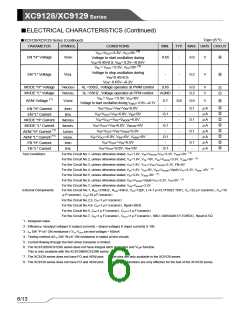
-
-
-
-
-
-
0
400
-
%
mA
%
④
①
①
⑤
⑦
Connect to external components,
VMODE=0V, RL=330Ω
Connect to external components,
RL=33Ω
250
93
VIN=VLx=VOUT+50mV,
VFB=0.45×1.1 (*3)
LX SW "Pch" ON Resistance
LX SW "Nch" ON Resistance
0.20
0.35 (*1)
Ω
RLxN
VIN=VOUT=3.3V, Lx =50mV (*4)
0.20 (*1) 0.35 (*1)
Ω
LX Leak Current
Current Limit (*5)
ILXL
ILIM
VIN=VOUT= VLX, VFB=0V
VOUT>2.5V
-
1
-
μA
⑤
①
1.2
1.5
2.0
A
Time to stop oscillation during
RL=33Ω → 3.3Ω, VFO=L → H
Time to stop oscillation during
RL=33Ω → 3.3Ω
Integral Latch Time (XC9128) (*6)
Integral Latch Time (XC9129) (*6)
tLAT
tSS1
tSS2
-
1.7
-
3.5
5.3
-
ms
ms
ms
①
④
④
Time to start oscillation during VEN=0V
→ VIN at VIN = VOUT =3.3V, VFO=0V,
VFB=0.45×0.95
Soft-Start Time 1
10.5
0.04
VIN = VOUT =3.3V, VFO=0V,
VFB=0.45×0.95
Time to start oscillation during
Soft-Start Time 2 (*7)
0.02
VAEN/=VIN→0V.
VIN = VOUT =3.3V, VFO=0V,
VFB=0.45×0.8
Time to start oscillation during
VAEN/=VIN→0V
Soft-Start Time 3 (*7)
tSS3
1.7
5.3
10.5
ms
④
Thermal Shutdown
Temperature
TTSD
THYS
-
-
-
150
20
-
-
oC
oC
-
-
Hysteresis Width
-
V
IN =3.3V
Output Voltage Drop
Protection (*6)
VLVP
Voltage to stop oscillation during
1.3
1.48
1.56
V
⑥
VOUT=1.56V→1.3V
FO Output Current (*7)
FO Leakage Current (*7)
IFO_OUT
IFO_Leak
VIN =VOUT=3.3V, VFO=0.25V
1.3
-
1.7
0
2.2
1
mA
④
④
VIN = VOUT =3.3V, VEN=0V ,VFO=1V
μA
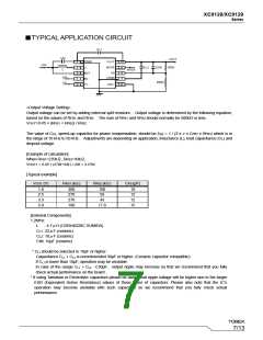
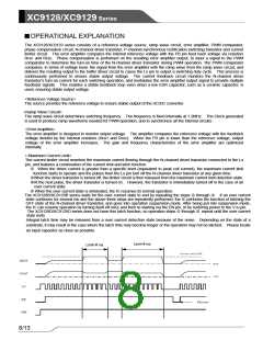
5/13

 TOREX [ Torex Semiconductor ]