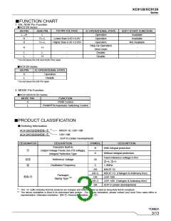
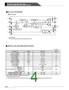
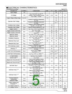
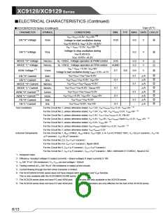
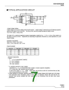
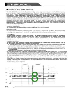
XC9128/XC9129 Series
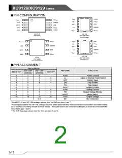
■PIN CONFIGURATION
6 AEN/
7 AGND
FO 5
EN 4
10 VOUT
9 MODE
8 FB
PGND
1
Lx 2
BAT 3
EN 4
FO 5
8 FB
BAT 3
9 MODE
Lx 2
7 AGND
6 AEN/
PGND
1
10 VOUT
MSOP-10
USP-10B
(TOP VIEW)
(BOTTOM VIEW)
XC9128 Series
8 VOUT
6 NC
NC 5
EN 4
PGND
1
7 AGND
7 MODE
6 FB
Lx 2
8 FB
BAT 3
9 MODE
Lx 2
BAT 3
EN 4
10 VOUT
PGND
1
5 AGND
USP-10B
SOP-8
(BOTTOM VIEW)
XC9129 Series
(TOP VIEW)
Under Development
■PIN ASSIGNMENT
PIN NUMBER
PIN NAME
FUNCTION
USP-10B*
(XC9128)
USP-10B*
(XC9129)
MSOP-10*
SOP-8 **
1
2
3
4
5
6
7
8
9
10
-
1
2
3
4
5
6
7
8
9
10
-
1
2
1
2
3
4
-
PGND
Lx
Power Ground
Output of Internal Power Switch
Battery Input
3
BAT
EN
4
Chip Enable
-
FO
Flag Output
-
-
AEN/
AGND
FB
Adaptor Enable
Analog Ground
7
5
6
7
8
-
8
Output Voltage Monitor
Mode Switch
9
MODE
VOUT
NC
10
5, 6
Output Voltage
No Connection
* For MSOP-10 and USP-10B packages, please short the GND pins (pins 1 and 7).
*The dissipation pad for the USP-10B package should be solder-plated following the recommended mount pattern and metal masking
so as to enhance mounting strength and heat release. If the pad needs to be connected to other pins, it should be connected to the
Ground pins (pins 1 and 7).
** For SOP-8 package, please short the GND pins (pins 1 and 5).
2/13

 TOREX [ Torex Semiconductor ]