UCD9090
www.ti.com
SLVSA30A –APRIL 2011–REVISED AUGUST 2011
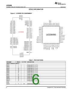
Table 1. PIN FUNCTIONS (continued)
PIN NAME
GPIO2
PIN NO.
I/O TYPE DESCRIPTION
5
I/O
I/O
I/O
I/O
I/O
I/O
I/O
I/O
General-purpose discrete I/O
General-purpose discrete I/O
General-purpose discrete I/O
General-purpose discrete I/O
General-purpose discrete I/O
General-purpose discrete I/O
General-purpose discrete I/O
General-purpose discrete I/O
GPIO3
6
GPIO4
7
GPIO13
18
21
24
25
26
GPIO14
GPIO15
GPIO16
GPIO17
PWM OUTPUTS
FPWM1/GPIO5
FPWM2/GPIO6
FPWM3/GPIO7
FPWM4/GPIO8
FPWM5/GPIO9
FPWM6/GPIO10
FPWM7/GPIO11
FPWM8/GPIO12
PWM1/GPI1
PWM2/GPI2
10
11
12
13
14
15
16
17
22
23
I/O/PWM
I/O/PWM
I/O/PWM
I/O/PWM
I/O/PWM
I/O/PWM
I/O/PWM
I/O/PWM
I/PWM
PWM (15.259 kHz to 125 MHz) or GPIO
PWM (15.259 kHz to 125 MHz) or GPIO
PWM (15.259 kHz to 125 MHz) or GPIO
PWM (15.259 kHz to 125 MHz) or GPIO
PWM (15.259 kHz to 125 MHz) or GPIO
PWM (15.259 kHz to 125 MHz) or GPIO
PWM (15.259 kHz to 125 MHz) or GPIO
PWM (15.259 kHz to 125 MHz) or GPIO
PWM (0.93 Hz to 7.8125 MHz) or GPI
PWM (0.93 Hz to 7.8125 MHz) or GPI
I/PWM
PMBus COMM INTERFACE
PMBUS_CLK
PMBUS_DATA
PMBUS_ALERT
PMBUS_CNTRL
PMBUS_ADDR0
PMBUS_ADDR1
JTAG
8
I/O
PMBus clock (must have pullup to 3.3 V)
PMBus data (must have pullup to 3.3 V)
9
I/O
19
20
44
43
O
I
PMBus alert, active-low, open-drain output (must have pullup to 3.3 V)
PMBus control
I
PMBus analog address input. Least-significant address bit
PMBus analog address input. Most-significant address bit
I
TCK/GPIO18
TDO/GPIO19
TDI/GPIO20
TMS/GPIO21
TRST
27
28
29
30
31
I/O
I/O
I/O
I/O
I
Test clock or GPIO
Test data out or GPIO
Test data in (tie to Vdd with 10-kΩ resistor) or GPIO
Test mode select (tie to Vdd with 10-kΩ resistor) or GPIO
Test reset – tie to ground with 10-kΩ resistor
INPUT POWER AND GROUNDS
RESET
V33A
3
Active-low device reset input. Hold low for at least 2 μs to reset the device.
Analog 3.3-V supply. Refer to the Layout Guidelines section.
Digital core 3.3-V supply. Refer to the Layout Guidelines section.
1.8-V bypass capacitor. Refer to the Layout Guidelines section.
Analog ground
34
33
35
36
47
32
NA
V33D
BPCap
AVSS1
AVSS2
DVSS
Analog ground
Digital ground
QFP ground pad
Thermal pad – tie to ground plane.
FUNCTIONAL DESCRIPTION
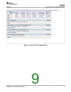
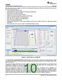
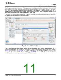
TI FUSION GUI
The Texas Instruments Fusion Digital Power Designer is provided for device configuration. This PC-based
Copyright © 2011, Texas Instruments Incorporated
7

 TI [ TEXAS INSTRUMENTS ]