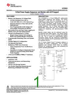
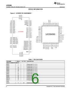
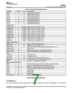
UCD9090
www.ti.com
SLVSA30A –APRIL 2011–REVISED AUGUST 2011
PMBus/SMBus/I2C
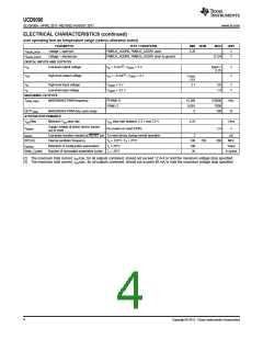
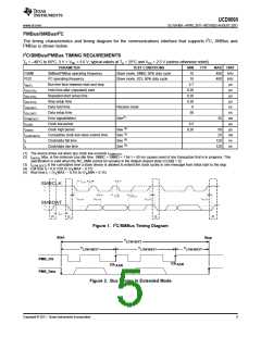
The timing characteristics and timing diagram for the communications interface that supports I2C, SMBus and
PMBus is shown below.
I2C/SMBus/PMBus TIMING REQUIREMENTS
TA = –40°C to 85°C, 3 V < VDD < 3.6 V; typical values at TA = 25°C and VCC = 2.5 V (unless otherwise noted)
PARAMETER
TEST CONDITIONS
Slave mode, SMBC 50% duty cycle
Slave mode, SCL 50% duty cycle
MIN
10
TYP
MAX UNIT
FSMB
FI2C
SMBus/PMBus operating frequency
I2C operating frequency
Bus free time between start and stop
Hold time after (repeated) start
Repeated-start setup time
Stop setup time
400
400
kHz
kHz
μs
10
t(BUF)
4.7
0.26
0.26
0.26
0
t(HD:STA)
t(SU:STA)
t(SU:STO)
t(HD:DAT)
t(SU:DAT)
t(TIMEOUT)
t(LOW)
μs
μs
μs
Data hold time
Receive mode
See(1)
ns
Data setup time
50
ns
Error signal/detect
35
ms
μs
Clock low period
0.5
(2)
t(HIGH)
t(LOW:SEXT)
tf
Clock high period
See
0.26
50
25
μs
(3)
Cumulative clock low slave extend time
Clock/data fall time
See
ms
ns
(4)
See
120
120
(5)
tr
Clock/data rise time
See
ns
(1) The device times out when any clock low exceeds t(TIMEOUT)
.
(2) t(HIGH), Max, is the minimum bus idle time. SMBC = SMBD = 1 for t > 50 ms causes reset of any transaction that is in progress. This
specification is valid when the NC_SMB control bit remains in the default cleared state (CLK[0] = 0).
(3) t(LOW:SEXT) is the cumulative time a slave device is allowed to extend the clock cycles in one message from initial start to the stop.
(4) Fall time tf = 0.9 VDD to (VILMAX – 0.15)
(5) Rise time tr = (VILMAX – 0.15) to (VIHMIN + 0.15)
Figure 1. I2C/SMBus Timing Diagram
Start
Stop
T
LOW:SEXT
T
T
T
LOW:MEXT
LOW:MEXT
LOW:MEXT
PMB_Clk
Clk
ACK
Clk
ACK
PMB_Data
Figure 2. Bus Timing in Extended Mode
Copyright © 2011, Texas Instruments Incorporated
5

 TI [ TEXAS INSTRUMENTS ]