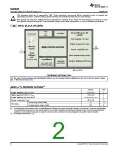
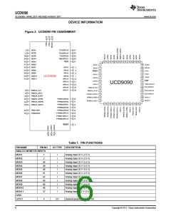
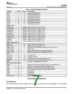
UCD9090
www.ti.com
SLVSA30A –APRIL 2011–REVISED AUGUST 2011
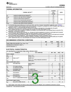
THERMAL INFORMATION
UCD9090
THERMAL METRIC(1)
RGZ
48 PINS
25
UNITS
θJA
Junction-to-ambient thermal resistance(2)
Junction-to-case (top) thermal resistance(3)
Junction-to-board thermal resistance(4)
Junction-to-top characterization parameter(5)
Junction-to-board characterization parameter(6)
Junction-to-case (bottom) thermal resistance(7)
θJCtop
θJB
8.9
5.5
°C/W
ψJT
0.3
ψJB
1.5
θJCbot
1.7
(1) For more information about traditional and new thermal metrics, see the IC Package Thermal Metrics application report, SPRA953.
(2) The junction-to-ambient thermal resistance under natural convection is obtained in a simulation on a JEDEC-standard, high-K board, as
specified in JESD51-7, in an environment described in JESD51-2a.
(3) The junction-to-case (top) thermal resistance is obtained by simulating a cold plate test on the package top. No specific
JEDEC-standard test exists, but a close description can be found in the ANSI SEMI standard G30-88.
(4) The junction-to-board thermal resistance is obtained by simulating in an environment with a ring cold plate fixture to control the PCB
temperature, as described in JESD51-8.
(5) The junction-to-top characterization parameter, ψJT, estimates the junction temperature of a device in a real system and is extracted
from the simulation data for obtaining θJA, using a procedure described in JESD51-2a (sections 6 and 7).
(6) The junction-to-board characterization parameter, ψJB, estimates the junction temperature of a device in a real system and is extracted
from the simulation data for obtaining θJA , using a procedure described in JESD51-2a (sections 6 and 7).
(7) The junction-to-case (bottom) thermal resistance is obtained by simulating a cold plate test on the exposed (power) pad. No specific
JEDEC standard test exists, but a close description can be found in the ANSI SEMI standard G30-88.
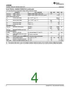
RECOMMENDED OPERATING CONDITIONS
MIN
3
NOM
MAX
3.6
UNIT
V
Supply voltage during operation (V33D, V33DIO, V33A
Operating free-air temperature range, TA
Junction temperature, TJ
)
3.3
–40
110
125
°C
°C
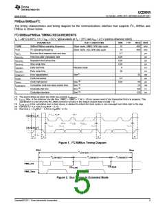
ELECTRICAL CHARACTERISTICS
over operating free-air temperature range (unless otherwise noted)
PARAMETER
TEST CONDITIONS
MIN NOM
MAX
UNIT
SUPPLY CURRENT
IV33A
VV33A = 3.3 V
VV33DIO = 3.3 V
VV33D = 3.3 V
8
2
mA
mA
mA
IV33DIO
Supply current(1)
IV33D
IV33D
ANALOG INPUTS (MON1–MON13)
40
VV33D = 3.3 V, storing configuration parameters in
flash memory
50
mA
VMON
Input voltage range
MON1–MON10
0
0.2
–4
-2
2.5
2.5
4
V
V
MON11
INL
ADC integral nonlinearity
ADC differential nonlinearity
Input leakage current
Input offset current
LSB
LSB
nA
DNL
Ilkg
2
3 V applied to pin
100
5
IOFFSET
1-kΩ source impedance
MON1–MON10, ground reference
MON11, ground reference
–5
8
μA
MΩ
MΩ
pF
RIN
Input impedance
0.5
1.5
3
CIN
Input capacitance
10
tCONVERT
ADC sample period
12 voltages sampled, 3.89 μsec/sample
0°C to 125°C
400
μsec
%
ADC 2.5 V, internal reference accuracy
–0.5
–1
0.5
1
VREF
–40°C to 125°C
%
ANALOG INPUT (PMBUS_ADDRx)
IBIAS Bias current for PMBus Addr pins
9
11
μA
(1) Typical supply current values are based on device programmed but not configured, and no peripherals connected to any pins.
Copyright © 2011, Texas Instruments Incorporated
3

 TI [ TEXAS INSTRUMENTS ]