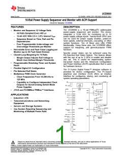
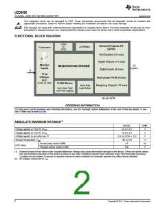
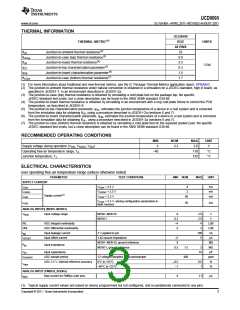
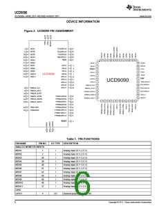
UCD9090
SLVSA30A –APRIL 2011–REVISED AUGUST 2011
www.ti.com
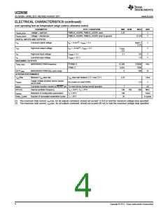
ELECTRICAL CHARACTERISTICS (continued)
over operating free-air temperature range (unless otherwise noted)
PARAMETER
Voltage – open pin
Voltage – shorted pin
TEST CONDITIONS
MIN NOM
MAX
UNIT
V
VADDR_OPEN
VADDR_SHORT
PMBUS_ADDR0, PMBUS_ADDR1 open
2.26
PMBUS_ADDR0, PMBUS_ADDR1 short to ground
0.124
V
DIGITAL INPUTS AND OUTPUTS
VOL
Low-level output voltage
IOL = 6 mA(2), V33DIO = 3 V
Dgnd +
0.25
V
V
VOH
High-level output voltage
IOH = –6 mA(3), V33DIO = 3 V
V33DIO
– 0.6
VIH
VIL
High-level input voltage
Low-level input voltage
V33DIO = 3 V
2.1
3.6
1.4
V
V
V33DIO = 3.5 V
MARGINING OUTPUTS
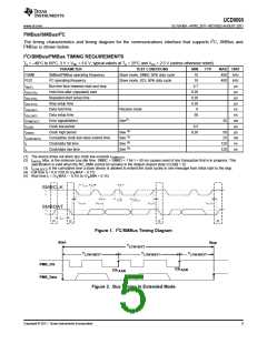
TPWM_FREQ MARGINING-PWM frequency
FPWM1-8
PWM1-2
15.260
0.001
0
125000
7800
100
kHz
%
DUTYPWM
MARGINING-PWM duty cycle range
SYSTEM PERFORMANCE
VDDSlew
VRESET
Minimum VDD slew rate
VDD slew rate between 2.3 V and 2.9 V
For power-on reset (POR)
0.25
V/ms
V
Supply voltage at which device comes
out of reset
2.4
tRESET
Low-pulse duration needed at RESET pin To reset device during normal operation
2
240
100
20
μS
MHz
f(PCLK)
tretention
Internal oscillator frequency
TA = 125°C, TA = 25°C
TJ = 25°C
250
260
Retention of configuration parameters
Years
K cycles
Write_Cycles
Number of nonvolatile erase/write cycles TJ = 25°C
(2) The maximum total current, IOLmax, for all outputs combined, should not exceed 12 mA to hold the maximum voltage drop specified.
(3) The maximum total current, IOHmax, for all outputs combined, should not exceed 48 mA to hold the maximum voltage drop specified.
4
Copyright © 2011, Texas Instruments Incorporated

 TI [ TEXAS INSTRUMENTS ]