UCD9090
SLVSA30A –APRIL 2011–REVISED AUGUST 2011
www.ti.com
This integrated circuit can be damaged by ESD. Texas Instruments recommends that all integrated circuits be handled with
appropriate precautions. Failure to observe proper handling and installation procedures can cause damage.
ESD damage can range from subtle performance degradation to complete device failure. Precision integrated circuits may be more
susceptible to damage because very small parametric changes could cause the device not to meet its published specifications.
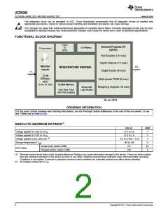
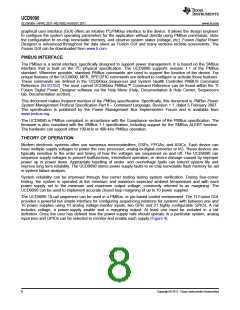
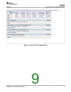
FUNCTIONAL BLOCK DIAGRAM
JTAG
Or
GPIO
General Purpose I/O
(GPIO)
I2C/PMBus
Comparators
Rail Enables (10 max)
6
Digital Outputs (10 max)
Digital Inputs (8 max)
Monitor
Inputs
23
SEQUENCING ENGINE
11
12-bit
200ksps,
Multi-phase PWM (8 max)
Margining Outputs (10 max)
ADC
(0.5% Int. Ref)
FLASH Memory
BOOLEAN
Logic Builder
User Data, Fault
and Peak Logging
48-pin QFN
ORDERING INFORMATION
For the most current package and ordering information, see the Package Option Addendum at the end of this document, or see
the TI Web site at www.ti.com.
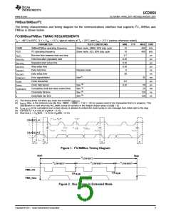
ABSOLUTE MAXIMUM RATINGS(1)
VALUE
–0.3 to 3.8
–0.3 to 3.8
–0.3 to (V33A + 0.3)
–40 to 150
2.5
UNIT
V
Voltage applied at V33D to DVSS
Voltage applied at V33A to AVSS
V
(2)
Voltage applied to any other pin
V
Storage temperature (Tstg
)
°C
kV
V
Human-body model (HBM)
ESD rating
Charged-device model (CDM)
750
(1) Stresses beyond those listed under Absolute Maximum Ratings may cause permanent damage to the device. These are stress ratings
only and functional operation of the device at these or any other conditions beyond those indicated under Recommended Operating
Conditions is not implied. Exposure to absolute-maximum-rated conditions for extended periods may affect device reliability.
(2) All voltages referenced to VSS
2
Copyright © 2011, Texas Instruments Incorporated

 TI [ TEXAS INSTRUMENTS ]