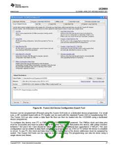
UCD9090
www.ti.com
SLVSA30A –APRIL 2011–REVISED AUGUST 2011
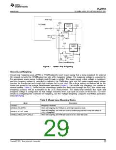
BROWNOUT FUNCTION
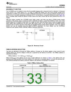
The UCD9090 can be enabled to turn off all nonvolatile logging until a brownout event is detected. A brownout
event occurs if VCC drops below 2.9 V. In order to enable this feature, the user must provide enough local
capacitance to deliver up to 80 mA (consider additional load based on GPOs sourcing external circuits such as
LEDs) on for 5 ms while maintaining a minimum of 2.6 V at the device. If using the brownout circuit (Figure 26),
then a schottky diode should be placed so that it blocks the other circuits that are also powered from the 3.3V
supply.
With this feature enabled, the UCD9090 saves faults, peaks, and other log data to SRAM during normal
operation of the device. Once a brownout event is detected, all data is copied from SRAM to Flash. Use of this
feature allows the UCD9090 to keep track of a single run-time clock that spans device resets or system power
down (rather than resetting the run time clock after device reset). It can also improve the UCD9090 internal
response time to events, because Flash writes are disabled during normal system operation. This is an optional
feature and can be enabled using the MISC_CONFIG command. For more details, see the UCD90xxx
Sequencer and System Health Controller PMBus Command Reference.
UCD9090
B340A
V33A
V33D
AVSS1
AVSS2
3.3V
C
DVSS
Figure 26. Brownout Circuit
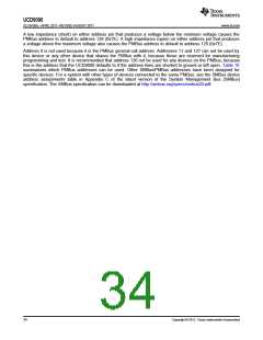
PMBUS ADDRESS SELECTION
Two pins are allocated to decode the PMBus address. At power up, the device applies a bias current to each
address-detect pin, and the voltage on that pin is captured by the internal 12-bit ADC. The PMBus address is
calculated as follows.
PMBus Address = 12 × bin(VAD01) + bin(VAD00
)
Where bin(VAD0x) is the address bin for one of eight addresses as shown in Table 9. The address bins are
defined by the MIN and MAX VOLTAGE RANGE (V). Each bin is a constant ratio of 1.25 from the previous bin.
This method maintains the width of each bin relative to the tolerance of standard 1% resistors.
Table 9. PMBus Address Bins
RPMBus
ADDRESS BIN
PMBus RESISTANCE (kΩ)
open
11
10
9
—
200
154
118
90.9
69.8
53.6
41.2
31.6
—
8
7
6
5
4
short
Copyright © 2011, Texas Instruments Incorporated
33

 TI [ TEXAS INSTRUMENTS ]