UCD9090
SLVSA30A –APRIL 2011–REVISED AUGUST 2011
www.ti.com
MON(1:10)
3.3V
UCD9090
POWER
SUPPLY
Vout
10kW
GPIO
/EN
VOUT
VFB
R1
R2
250 kHz – 1MHz
Vmarg
V
FB
FPWM1
R3
R4
C1
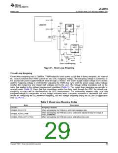
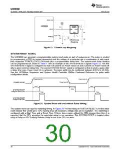
Closed Loop
Margining
Figure 22. Closed-Loop Margining
SYSTEM RESET SIGNAL
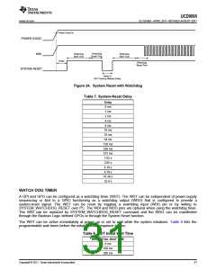
The UCD9090 can generate a programmable system-reset pulse as part of sequence-on. The pulse is created
by programming a GPIO to remain deasserted until the voltage of a particular rail or combination of rails reach
their respective POWER_GOOD_ON levels plus a programmable delay time. The system-reset delay duration
can be programmed as shown in Table 7. See an example of two SYSTEM RESET signals Figure 23. The first
SYSTEM RESET signal is configured so that it de-asserts on Power Good On and it asserts on Power Good Off
after a given common delay time. The second SYSTEM RESET signal is configured so that it sends a pulse after
a delay time once Power Good On is achieved. The pulse width can be configured between 0.001s to 32.256s.
See the UCD90xxx Sequencer and System Health Controller PMBus Command Reference for pulse width
configuration details.
Power Good On
Power Good On
Power Good Off
POWER GOOD
Delay
Delay
Delay
SYSTEM RESET
configured without pulse
Pulse
Pulse
SYSTEM RESET
configured with pulse
Figure 23. System Reset with and without Pulse Setting
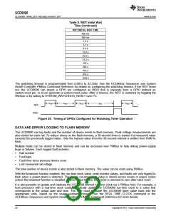
The system reset can react to watchdog timing. In Figure 24 The first delay on SYSTEM RESET is for the initial
reset release that would get a CPU running once all necessary voltage rails are in regulation. The watchdog is
configured with a Start Time and a Reset Time. If these times expire without the WDI clearing them then it is
expected that the CPU providing the watchdog signal is not operating. The SYSTEM RESET is toggled either
using a Delay or GPI Tracking Release Delay to see if the CPU recovers.
30
Copyright © 2011, Texas Instruments Incorporated

 TI [ TEXAS INSTRUMENTS ]