UCD9090
www.ti.com
SLVSA30A –APRIL 2011–REVISED AUGUST 2011
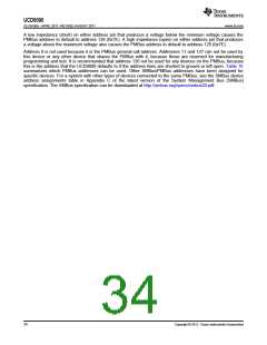
Table 10. PMBus Address Assignment Rules
Address
STATUS
Prohibited
Avoid
Reason
0
SMBus generaladdress call
11
Causes conflicts with other devices during program flash updates.
PMBus alert response protocol
12
Prohibited
For JTAG Use
Prohibited
126
127
Default value; may cause conflicts with other devices.
Used by TI manufacturing for device tests.
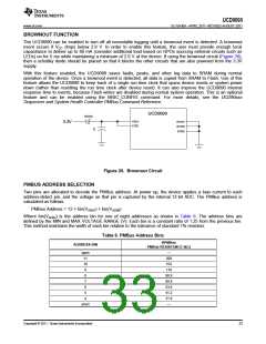
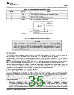
VDD
UCD9090
10uA
On/Off Control
Ibias
To 12-bit ADC
PMBUS_ADDR0
PMBUS_ADDR1
Resistors to set
PMBus address
Figure 27. PMBus Address-Detection Method
CAUTION
Address 126 (0x7E) is not recommended to be selected as a permanent PMBus
address for any given application design. Leaving the address in default state as 126
(0x7E) will enable the JTAG and not allow using the JTAG compatible pins (27-30) as
GPIOs. The UCD9090 runs at 10% slower frequency while the JTAG is enabled to
ensure best JTAG operation.
DEVICE RESET
The UCD9090 has an integrated power-on reset (POR) circuit which monitors the supply voltage. At power up,
the POR detects the V33D rise. When V33D is greater than VRESET, the device comes out of reset.
The device can be forced into the reset state by an external circuit connected to the RESET pin. A logic-low
voltage on this pin for longer than tRESET holds the device in reset. It comes out of reset within 1 ms after
RESETis released and can return to a logic-high level. To avoid an erroneous trigger caused by noise, connect
RESET to a 10kohm pullup resistor (from RESET to 3.3 V) and a 1000pF capacitor (from RESET to AVSS).
Any time the device comes out of reset, it begins an initialization routine that lasts about 20 ms. During the
initialization routine, the FPWM pins are held low, and all other GPIO and GPI pins are open-circuit. At the end of
initialization, the device begins normal operation as defined by the device configuration.
DEVICE CONFIGURATION AND PROGRAMMING
From the factory, the device contains the sequencing and monitoring firmware. It is also configured so that all
GPOs are high-impedance (except for FPWM/GPIO pins 10-17, which are driven low), with no sequencing or
fault-response operation. See Configuration Programming of UCD Devices, available from the Documentation &
Help Center that can be selected from the Fusion GUI Help menu, for full UCD9090 configuration details.
After the user has designed a configuration file using Fusion GUI, there are three general device-configuration
programming options:
1. Devices can be programmed in-circuit by a host microcontroller using PMBus commands over I2C (see the
UCD90xxx
Sequencer
and
System
Health
Controller
PMBus
Command
Reference).
Each parameter write replaces the data in the associated memory (RAM) location. After all the required
configuration data has been sent to the device, it is transferred to the associated nonvolatile memory (data
flash) by issuing a special command, STORE_DEFAULT_ALL. This method is how the Fusion GUI normally
Copyright © 2011, Texas Instruments Incorporated
35

 TI [ TEXAS INSTRUMENTS ]