UCD8220, UCD8620
www.ti.com
SLUS652B–MARCH 2005–REVISED SEPTEMBER 2005
Selecting the ISET Resistor for Voltage Mode
Control
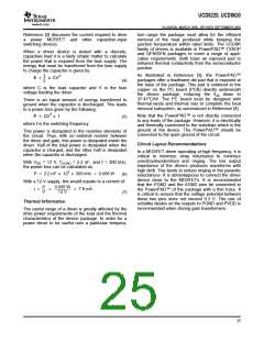
Figure 45 shows the nominal value of resistance to
use for a desired clock frequency. Note that for the
UCD8220 and the UCD8620 controllers, which have
two outputs controlled by Push-Pull logic, the output
ripple frequency is equal to the clock frequency; and
each output switches at half the clock frequency.
3V3
3V3
(3)
R_ISET
ISET
I_SC = (3.3 - 1.85) / (11 x R_ISET)
(4)
Selecting the ISET Resistor for Voltage Mode
Control with Voltage Feed forward
R
PWM
CTRL
(6)
-
3V3
TO CLEAR
of
VIN
+
R
PWM LATCH
0.25 V
R_ISET
C
int
ISET
S1
OUT
9.4 pF
I_SC = (3.3 - 1.85) / (11 x R_ISET)
(4)
ON
OFF
R
PWM
CTRL
(6)
-
TO CLEAR
of
+
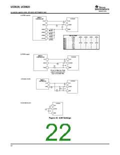
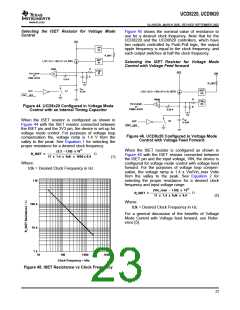
Figure 44. UCD8x20 Configured in Voltage Mode
Control with an Internal Timing Capacitor
R
PWM LATCH
0.25 V
C
int
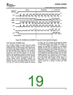
When the ISET resistor is configured as shown in
Figure 44 with the ISET resistor connected between
the ISET pin and the 3V3 pin, the device is set-up for
voltage mode control. For purposes of voltage loop
compensation the, voltage ramp is 1.4 V from the
valley to the peak. See Equation 1 for selecting the
proper resistance for a desired clock frequency.
S1
OUT
9.4 pF
ON OFF
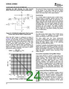
Figure 46. UCD8x20 Configured in Voltage Mode
Control with Voltage Feed Forward
12
When the ISET resistor is configured as shown in
Figure 46 with the ISET resistor connected between
the ISET pin and the input voltage, VIN, the device is
configured for voltage mode control with voltage feed
forward. For the purposes of voltage loop compen-
sation, the voltage ramp is 1.4 x Vin/Vin_max Volts
from the valley to the peak. See Equation 2 for
selecting the proper resistance for a desired clock
frequency and input voltage range.
(3.3 - 1.85) x 10
W
R_ISET =
11 x 1.4 x fclk x 1000 x 9.4
(1)
Where:
fclk = Desired Clock Frequency in Hz.
1 M
100 k
10 k
1 k
12
(Vin_max - 1.85) x 10
W
R_ISET =
11 x 1.4 x fclk x 9.4
(2)
Where:
fclk = Desired Clock Frequency in Hz.
For a general discussion of the benefits of Voltage
Mode Control with Voltage feed forward, see Refer-
ence [5].
10
100
1000
10000
Clock Frequency − kHz
Figure 45. ISET Resistance vs Clock Frequency
23

 TI [ TEXAS INSTRUMENTS ]