UCD8220, UCD8620
www.ti.com
SLUS652B–MARCH 2005–REVISED SEPTEMBER 2005
(1) For VDD to go below 12 V, the input supply must be dropping out.
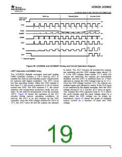
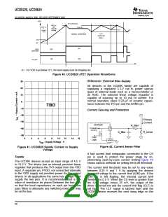
Figure 40. UCD8620 JFET Operation Waveforms
Reference / External Bias Supply
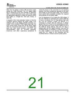
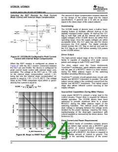
30
20
10
0
All devices in the UCD8K family are capable of
supplying a regulated 3.3-V rail to power various
types of external loads such as a microcontroller or
an ASIC. The onboard linear voltage regulator is
capable of sourcing up to 10 mA of current. For
normal operation, place 0.22-µF of ceramic capaci-
tance between the 3V3 pin and the AGND pin.
TBD
−10
−20
−30
Current Sensing and Protection
−40
−50
0
2
4
6
8
10
12
14
16
V
- Supply Voltage - V
DD
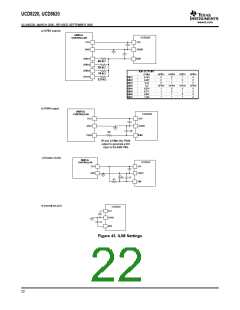
Figure 42. Current Sense Filter
Figure 41. UCD8620 Supply Current vs Supply
Voltage
A fast current limit comparator connected to the CS
pin is used to protect the power stage by im-
plementing cycle-by-cycle current limiting.Figure 43
shows various methods for setting the ILIM threshold.
Supply
The UCD8K devices accept an input range of 4.5 V
to 15.5 V. The device has an internal precision linear
regulator that produces the 3V3 output from this VDD
input. A separate pin, PVDD, not connected internally
to the VDD supply rail provides power for the output
drivers. In all applications the same bus voltage must
supply the two pins. It is recommended that a low
value of resistance be placed between the two pins
so that the local capacitance on each pin forms low
pass filters to attenuate any switching noise that may
be on the bus.
The current limit threshold may be set to any value
between 0.25 V and 1 V by applying the desired
threshold voltage to the current limit (ILIM) pin. If the
ILIM pin is left floating, the internal current limit
threshold is 0.5 V. When the CS level is greater than
the ILIM voltage minus 25 mV, the output of the
driver is forced low and the current limit flag (CLF) is
set high. The CLF signal is latched high until the
UCD8K device receives the next rising edge on the
CLK pin.
20

 TI [ TEXAS INSTRUMENTS ]