UCD8220, UCD8620
www.ti.com
SLUS652B–MARCH 2005–REVISED SEPTEMBER 2005
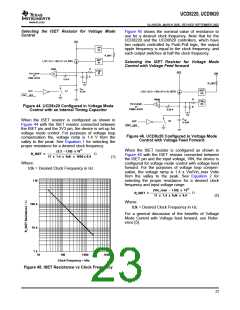
Selecting the ISET Resistor for Peak Current
Mode Control with Internal Slope Compensation
The amount of slope compensation required depends
on the design of the power stage and the output
specifications. A general rule is to add an up-slope
equal to the down slope of the output inductor.
3V3
ISET
I_SC = 1.85 / (11 x R_ISET)
(4)
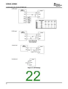
Handshaking
R_ISET
R
The UCD8K family of devices have a built-in hand-
shaking feature to facilitate efficient start-up of the
digitally managed power supply. At start-up the CLF
flag is held high until all the internal and external
supply voltages of the UCD8K device are within their
operating range. Once the supply voltages are within
acceptable limits, the CLF goes low and the device
processes the CLK signals. The digital controller
should monitor the CFL flag at start-up and wait for
the CLF flag to go LOW before sending CLK pulses
to the UCD8K device.
PWM
CTRL
-
TO CLEAR
of
(6)
+
R
PWM LATCH
0.25 V
C
int
S1
OUT
12 pF
ON
OFF
CS
(9)
S2
Driver Output
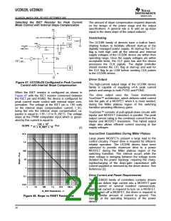
Figure 47. UCCD8x20 Configured in Peak Current
Control with Internal Slope Compensation
The high-current output stage of the UCD8K device
family is capable of supplying ±4-A peak current
pulses and swings to both PVDD and PGND.
When the ISET resistor is configured as shown in
Figure 47 with the ISET resistor connected between
the ISET pin and AGND, the device is configured for
peak current mode control with internal slope com-
pensation. The voltage at the ISET pin is 1.85 volts
so the internal slope compensation current, I_SC,
being fed into the internal slope compensation ca-
pacitor is equal to 1.85 / (11x R_ISET). The voltage
slope at the PWM comparator input which is gener-
ated by this current is equal to:
The drive output uses the Texas Instruments
TrueDrive™ architecture, which delivers rated current
into the gate of a MOSFET when it is most needed,
during the Miller plateau region of the switching
transition providing efficiency gains.
TrueDrive™ consists of pull-up/pull-down circuits with
bipolar and MOSFET transistors in parallel. The peak
output current rating is the combined current from the
bipolar and MOSFET transistors. This hybrid output
stage also allows efficient current sourcing at low
supply voltages.
6
1.85 x 10
V/ms
SLOPE =
11 x R_ISET x 12
(3)
Source/Sink Capabilities During Miller Plateau
10 k
Large power MOSFETs present a large load to the
control circuitry. Proper drive is required for efficient,
reliable operation. The UCD8K drivers have been
optimized to provide maximum drive to a power
MOSFET during the Miller plateau region of the
switching transition. This interval occurs while the
drain voltage is swinging between the voltage levels
dictated by the power topology, requiring the charg-
ing/discharging of the drain-gate capacitance with
current supplied or removed by the driver device. See
Reference [2].
1 k
100
10
1
Drive Current and Power Requirements
0.1
The UCD8620 family of controllers contains drivers
which can deliver high current into a MOSFET gate
0.01
for
a period of several hundred nanoseconds.
1
10
100
1 k
10 k
100 k 1 M
High-peak current is required to turn on a MOSFET.
Then, to turn off a MOSFET, the driver is required to
sink a similar amount of current to ground. This
repeats at the operating frequency of the power
device.
R_ISET Resistance - W
Figure 48. Slope vs RISET Resistance
24

 TI [ TEXAS INSTRUMENTS ]