UCD8220, UCD8620
www.ti.com
SLUS652B–MARCH 2005–REVISED SEPTEMBER 2005
Start up
Steady State
Current Limit
UVLO and
REF OK*
CLK
CTRL
RAMP*
PWM*
OUT
CS
CLF
* - Internal signals
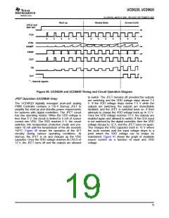
Figure 39. UCD8220 and UCD8620 Timing and Circuit Operation Diagram
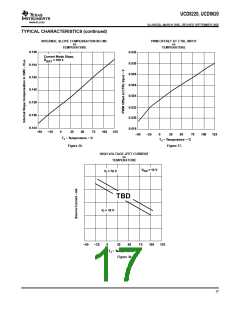
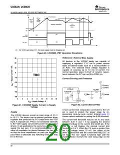
to switch. The JFET remains off provided the outputs
are switching and the VDD voltage stays above 7.5
V. If the VDD voltage drops below 7.5 V while the
outputs are switching, the outputs are immediately
disabled, and the JFET is switched back on. It then
attempts to charge the VDD voltage back up to 13 V.
Once the VDD voltage reaches 13 V, the outputs are
enabled again and allowed to switch. If the CLK input
is not switched by the digital controller, then the VDD
voltage decays to 12 V, and the JFET turns on again.
This charges the VDD capacitor back to 13 V where
the cycle repeats until the input voltage drops to a
point where the VDD voltage can no longer be
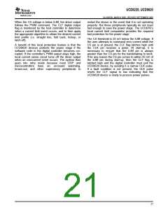
maintained. Figure 41 shows the graph of available
source current as a function of input and VDD
voltage.
JFET Operation (UCD8620 Only)
The UCD8620 digitally managed push-pull analog
PWM Controller contains a 110-V start-up JFET to
simplify the start-up and standby power requirements
for systems with digital controllers. The JFET circuit
has two operating modes. When the VDD voltage is
less than 5 V, the circuit is limited to 5 mA of source
current into VDD. The VDD reaches 5 V, the circuit
switches into temperature protection mode and pro-
vides 10 mA until the temperature of the die exceeds
145°C. Figure 40 shows the operation of the JET
circuitry during various operating conditions. At
start-up, the JFET is on and charges up the VDD
capacitor. Once the VDD voltage reaches its UVLO of
13 V, the JFET turns off and the outputs are allowed
19

 TI [ TEXAS INSTRUMENTS ]