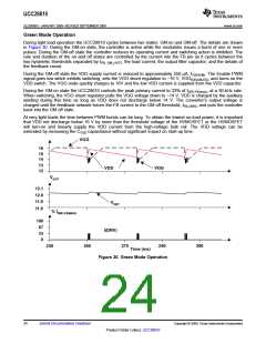
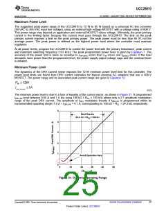
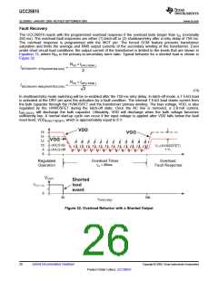
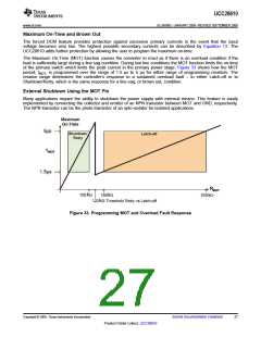
UCC28610
SLUS888C–JANUARY 2009–REVISED SEPTEMBER 2009 ......................................................................................................................................... www.ti.com
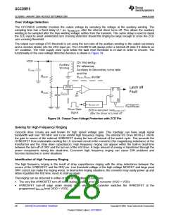
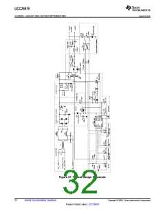
Over Voltage Detection
The UCC28610 controller monitors the output voltage by sampling the voltage at the auxiliary winding. The
sampling time has a fixed delay of 1 µs, tBLANK,OVP, after the internal driver turns off. This allows the auxiliary
winding to be sampled after the bias winding voltage settles from the transient. This same delay is used to blank
the ZCD input to avoid unintended zero crossing detection should the ringing be large enough to cross the ZCD
zero crossing threshold.
The output over-voltage (OV) threshold is set using the turn ratio of the auxiliary winding to the output secondary
and a resistive divider into the ZCD input pin. The UCC28610 will always enter a latched-off state if it detects an
OV condition. The VDD supply must cycle below the fault reset threshold to re-start in order to recover. The
functionality of the over-voltage detection function is shown in Figure 34.
Figure 34. Output Over-Voltage Protection with ZCD Pin
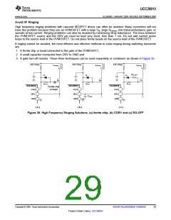
Solving for High Frequency Ringing
Cascode drive circuits are well known for high speed voltage gain. This topology can have small signal
bandwidth well over 100 MHz and it can exhibit high frequency ringing. The internal HS Drive MOSFET shorts
the gate to source of the external HVMOSFET during the turn-off interval of the switch cycle. This prevents the
HVMOSFET from undesirably exciting the LC resonant circuit in the converter (the magnetizing inductance of the
transformer and the stray drain capacitance). High frequency ringing can appear within the built-in dead-time
between the turn-off of DRV and the turn-on of the HS Drive. A large amount of energy is transferred through the
power components during this dead-time. Excessive high frequency ringing can cause EMI problems and
become destructive in some situations.
Identification of High Frequency Ringing
The high frequency ringing is the result of stray capacitances ringing with the stray inductance between the
source of the HVMOSFET and the DRV pin. Low threshold voltage of the high voltage MOSFET and large peak
DRV current can make the ringing worse. In destructive ringing situations, the converter may easily power up and
attain regulation the first time, never to start-up again.
The ringing can be observed in either or both of the following conditions:
•
•
The very first HVMOSFET turn-off event during a cold start of the converter (VGG > VDD).
HVMOSFET turn-off edge under steady state, where the converter switches the HVMOSFET at the
programmed IDRV,PK level (VDD > VGG).
28
Submit Documentation Feedback
Copyright © 2009, Texas Instruments Incorporated
Product Folder Link(s): UCC28610

 TI [ TEXAS INSTRUMENTS ]