UCC28610
SLUS888C–JANUARY 2009–REVISED SEPTEMBER 2009 ......................................................................................................................................... www.ti.com
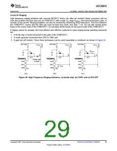
Ferrite Chip or Bead Solution
The ferrite chip or bead connected to the gate of the HVMOSFET provides the best result because it suppresses
ringing in the gate, source, and drain circuits of the HVMOSFET with minimal added losses. Select the ferrite
chip for its resistance value in the ringing frequency range (for example, 60 Ω at 100 MHz). The peak current
rating of the ferrite chip or bead must be sufficient for the drain – gate discharge current that occurs during the
turn-off transient. Excessively large bead reactance can result in low frequency surges of VGG at peak load.
Normally, good results can be achieved with a 0603 ferrite chip device.
DRV Capacitor Solution
A capacitor between DRV and GND can reduce ringing on VGG. Select the DRV capacitor experimentally by
observing the effect on the VGG pin during the first turn-off edge and during the turn-off edge at full load
operation. The capacitor should be less than 3.3 nF so that it does not significantly reduce efficiency. Use a
capacitor with a low Q, such as one with Y5V dielectric. This technique will not completely damp the ringing yet it
can provide sufficient protection against stray inductance between the source of the HVMOSFET and the DRV
pin.
Gate Turn-Off Resistor Solution
A gate turn-off resistor in the range 0 Ω < RG-OFF < 5 Ω can damp ringing. The turn-off resistance is limited in
order to prevent the stray source inductance of the HVMOSFET from over charging VGG through the body diode
of the HS Drive MOSFET, in addition to any peak current error problems that would be caused by additional
delay. The damping effect of the gate resistor works better in applications with low current and small source
inductance.
A much larger resistance can be tolerated during the HVMOSFET turn-on transition due to DCM operation. The
recommended turn-on resistance range is 0 Ω <RG-ON < 200 Ω in order to prevent the turn-on delay from
interfering with valley switching.
Thermal Shutdown
The UCC28610 protects itself from overheating with an internal thermal shutdown circuit. If the junction
temperature exceeds the thermal shutdown point, TSD, the UCC28610 initiates a shutdown event and permits
retry after the retry time, tRETRY. Shutdown/Retry cycles continue if the junction temperature is not less than TSD
minus TSD_HYST
.
30
Submit Documentation Feedback
Copyright © 2009, Texas Instruments Incorporated
Product Folder Link(s): UCC28610

 TI [ TEXAS INSTRUMENTS ]