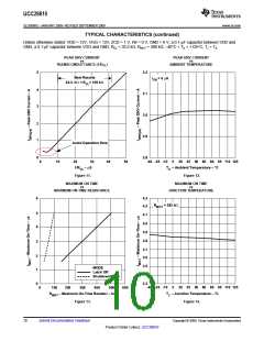
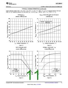
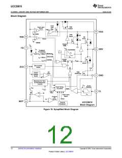
UCC28610
SLUS888C–JANUARY 2009–REVISED SEPTEMBER 2009 ......................................................................................................................................... www.ti.com
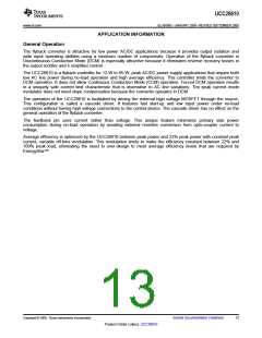
Transformer Selection
To begin a power supply design, the power supply designer needs to know the peak power to be delivered by
the converter, the input voltage range, the output voltage, and an estimate of the maximum allowable bulk
voltage ripple. Select the maximum allowable stress voltage for the external power MOSFET. The stress voltage
determines the reflected secondary voltage that resets the flyback transformer and the turn ratio between primary
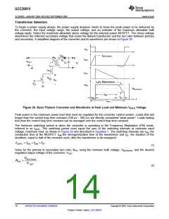
and secondary. A simplified diagram of the converter and its waveforms are shown in Figure 20.
NPS
Figure 20. Basic Flyback Converter and Waveforms at Peak Load and Minimum VBULK Voltage
Peak power is the maximum power level that must be regulated by the converter control system. Loads that last
longer than the control loop time constant (100 µs - 300 µs) are directly considered “peak power”. Loads lasting
less than the control loop time constant can be averaged over the control loop time constant.
The minimum switching period is when the converter is operating in the Frequency Modulation (FM) mode,
referred to as tS(HF). This switching period must equal the sum of the switching intervals at minimum input
voltage, maximum load, as shown in Figure 20 and described in Equation 1. The switching intervals are tON, the
conduction time of the MOSFET; tDM the demagnetization time of the transformer and tDT, the duration of the
deadtime, equal to half of the resonant cycle, after the transformer is de-energized.
tS( HF ) = tON + tDM + tDT
(1)
Solve for the primary to secondary turn ratio, NPS, using the minimum bulk voltage, VBULK(min), and the desired
regulated output voltage of the converter, VOUT
.
VBULK(min)
NPS
=
V OUT
(2)
14
Submit Documentation Feedback
Copyright © 2009, Texas Instruments Incorporated
Product Folder Link(s): UCC28610

 TI [ TEXAS INSTRUMENTS ]