UCC28951
www.ti.com.cn
ZHCSIQ7A –AUGUST 2018 –REVISED DECEMBER 2021
The voltage amplifier reference voltage (Pin 2, EA +) can be set with a voltage divider (R1, R2), for this design
example, the error amplifier reference voltage (V1) will be set to 2.5 V. Select a standard resistor value for R1
and then calculate resistor value R2.
UCC28951 reference voltage:
VREF = 5V
(110)
Set voltage amplifier reference voltage:
V1= 2.5V
(111)
(112)
R1= 2.37kW
R1´ V - V1
(
)
REF
R2 =
= 2.37kW
V1
(113)
The voltage divider formed by resistor R3 and R4 are chosen to set the DC output voltage (VOUT) at Pin 3 (EA-).
Select a standard resistor for R3:
R3 = 2.37kW
(114)
(115)
(116)
Calculate R4 using 方程式115:
R3´ V - V1
(
)
OUT
R4 =
» 9kW
V1
Then choose a standard resistor for R4 using 方程式116:
R3´ V - V1
(
)
OUT
R4 =
» 9.09kW
V1
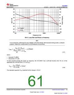
备注
TI recommends using an RCD clamp to protect the output synchronous FETs from overvoltage due to
switch node ringing.
Copyright © 2023 Texas Instruments Incorporated
Submit Document Feedback
57
Product Folder Links: UCC28951
English Data Sheet: SLUSDB2

 TI [ TEXAS INSTRUMENTS ]