UCC28951
www.ti.com.cn
ZHCSIQ7A –AUGUST 2018 –REVISED DECEMBER 2021
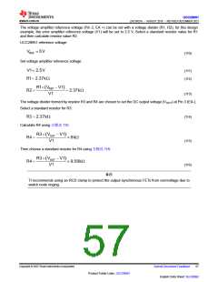
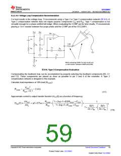
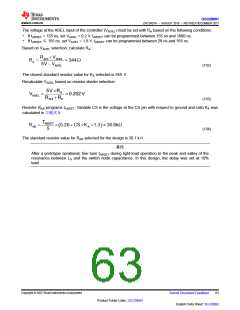
8.2.2.10.1 Voltage Loop Compensation Recommendation
For best results in the voltage loop, TI recommends using a Type 2 or Type 3 compensation network (图 8-6). A
Type 2 compensation network does not require passive components CZ2 and RZ2. Type 1 compensation is not
versatile enough for a phase-shifted full bridge. When evaluating the COMP pin for best results, TI recommends
placing a 1-kΩresistor between the scope probe and the COMP pin of the UCC28951.
VOUT
VREF
EA+
EA-
+
CZ2
RI
R
1 kW
RD
CZ1
RZ2
RZ1
CP1
R
When evaluating COMP, for best results put
a 1-kW resistor between COMP and probe.
图8-6. Type 3 Compensation Evaluation
Compensating the feedback loop can be accomplished by properly selecting the feedback components (R5, C1
and C2). These components are placed as close as possible to pin 3 and 4 of the controller. A Type 2
compensation network is designed in this example.
Calculate load impedance at 10% load (RLOAD) :
2
VOUT
RLOAD
=
= 2.4W
POUT ´0.1
(117)
Approximate control to output transfer function (GCO(f)) as a function of frequency:
æ
ç
è
ö
÷
ø
DVOUT
DVC
RLOAD
RCS
1+ 2pj´ f ´ESRCOUT ´COUT
1+ 2pj´ f ´RLOAD ´COUT
1
GCO(f) »
= a1´CTRAT
´
´
´
æ
ç
è
ö2
÷
S(f)
S(f)
2p´ fPP
1+
+
2p´ fPP
ø
(118)
Copyright © 2023 Texas Instruments Incorporated
Submit Document Feedback
59
Product Folder Links: UCC28951
English Data Sheet: SLUSDB2

 TI [ TEXAS INSTRUMENTS ]