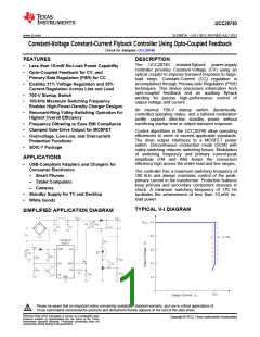
UCC28740
SLUSBF3A –JULY 2013–REVISED JULY 2013
www.ti.com
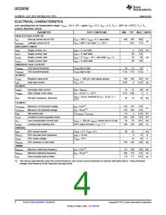
ELECTRICAL CHARACTERISTICS
over operating free-air temperature range, VVDD = 25 V, HV = open, VFB = 0 V, VVS = 4 V, TA = –40°C to +125°C, TJ = TA
(unless otherwise noted)
PARAMETER
HIGH-VOLTAGE START UP
TEST CONDITIONS
MIN
TYP MAX UNITS
IHV
Start-up current out of VDD
Leakage current at HV
VHV = 100 V, VVDD = 0 V, start state
VHV = 400 V, run state, TJ = 25°C
100 250
500
0.5
µA
IHVLKG25
0.01
BIAS SUPPLY INPUT
IRUN
Supply current, run
IDRV = 0, run state
2
95
18
95
2.65
125
30
mA
µA
IWAIT
ISTART
IFAULT
Supply current, wait
Supply current, start
Supply current, fault
IDRV = 0, wait state
IDRV = 0, VVDD = 18 V, start state, IHV = 0
IDRV = 0, fault state
130
UNDERVOLTAGE LOCKOUT
VVDD(on)
VVDD(off)
VS INPUT
VVSNC
VDD turnon threshold
VDD turnoff threshold
VVDD low to high
VVDD high to low
19
21
23
V
7.35 7.75
8.15
Negative clamp level
Input bias current
IVSLS = –300 µA, volts below ground
VVS = 4 V
190 250
325
mV
µA
IVSB
–0.25
16
0
0.25
FB INPUT
IFBMAX
Full-range input current
Input voltage at full range
fSW = fSW(min)
23
30
1
µA
V
VFBMAX
IFB = 25 µA, TJ = 25°C
0.75 0.88
ΔIFB = 20 µA, centered at IFB = 15 µA, TJ =
25°C
RFB
FB-input resistance, linearized
10 14
18
kΩ
CS INPUT
VCST(max)
VCST(min)
KAM
Maximum CS threshold voltage
Minimum CS threshold voltage
AM-control ratio
IFB = 0 µA(1)
IFB = 35 µA(1)
738 773
170 194
810
215
mV
VCST(max) / VCST(min)
3.6
318 330
24 25
180 230
4
4.45 V/V
343 mV
28.6 A/A
VCCR
Constant-current regulation factor
Line-compensation current ratio
Leading-edge blanking time
KLC
IVSLS = –300 µA, IVSLS / current out of CS pin
DRV output duration, V CS = 1 V
tCSLEB
280
ns
DRIVERS
IDRS
DRV source current
VDRV = 8 V, VVDD = 9 V
IDRV = 10 mA
20
25
6
mA
Ω
RDRVLS
VDRCL
DRV low-side drive resistance
DRV clamp voltage
12
16
VVDD = 35 V
14
V
RDRVSS
TIMING
fSW(max)
fSW(min)
tZTO
DRV pulldown in start-state
150 190
230
kΩ
Maximum switching frequency
Minimum switching frequency
Zero-crossing timeout delay
IFB = 0 µA(1)
IFB = 35 µA(1)
91 100
106 kHz
140 170
210
Hz
µs
1.8
2.1
2.55
(1) This device automatically varies the control frequency and current sense thresholds to improve EMI performance. These threshold
voltages and frequency limits represent average levels.
4
Submit Documentation Feedback
Copyright © 2013, Texas Instruments Incorporated
Product Folder Links: UCC28740

 TI [ TEXAS INSTRUMENTS ]