UCC28740
www.ti.com
SLUSBF3A –JULY 2013–REVISED JULY 2013
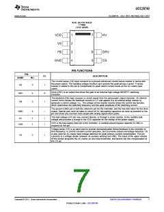
SOIC (D) PACKAGE
7 PINS
(TOP VIEW)
PIN FUNCTIONS
PIN
I/O
DESCRIPTION
NAME
NO.
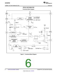
The current-sense (CS) input connects to a ground-referenced current-sense resistor in series with
the power switch. The resulting voltage monitors and controls the peak primary current. A series
resistor is added to this pin to compensate for peak switch-current levels as the AC-mains input
varies.
CS
5
I
O
I
Drive (DRV) is an output that drives the gate of an external high-voltage MOSFET switching
transistor.
DRV
FB
6
3
The feedback (FB) input receives a current signal from the optocoupler output transistor. An internal
current mirror divides the feedback current by 2.5 and applies it to an internal pullup resistor to
generate a control voltage, VCL. The voltage at this resistor directly drives the control law function,
which determines the switching frequency and the peak amplitude of the switching current .
The ground (GND) pin is both the reference pin for the controller, and the low-side return for the drive
output. Special care must be taken to return all AC-decoupling capacitors as close as possible to this
pin and avoid any common trace length with analog signal-return paths.
GND
4
—
The high-voltage (HV) pin may connect directly, or through a series resistor, to the rectified bulk
voltage and provides a charge to the VDD capacitor for the startup of the power supply.
HV
7
1
I
I
VDD is the bias-supply input pin to the controller. A carefully-placed bypass capacitor to GND is
required on this pin.
VDD
Voltage sense (VS) is an input used to provide demagnetization timing feedback to the controller to
limit frequency, to control constant-current operation, and to provide output-overvoltage detection. VS
is also used for AC-mains input-voltage detection for peak primary-current compensation. This pin
connects to a voltage divider between an auxiliary winding and GND. The value of the upper resistor
of this divider programs the AC-mains run and stop thresholds, and factors into line compensation at
the CS pin.
VS
2
I
Copyright © 2013, Texas Instruments Incorporated
Submit Documentation Feedback
7
Product Folder Links: UCC28740

 TI [ TEXAS INSTRUMENTS ]