UCC28740
SLUSBF3A –JULY 2013–REVISED JULY 2013
www.ti.com
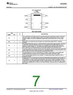
Detailed Pin Description
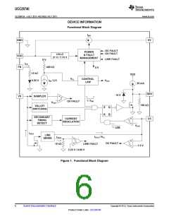
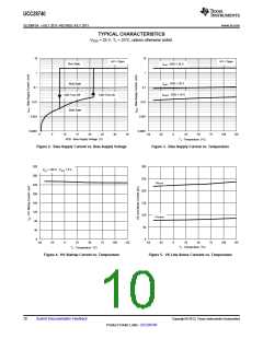
VDD (Device Bias Voltage Supply) The VDD pin connects to a bypass capacitor-to-ground. The turnon UVLO
threshold is 21 V and turnoff UVLO threshold is 7.75 V with an available operating range up to 35 V on
VDD. The typical USB-charging specification requires the output current to operate in constant-current
mode from 5 V down to at least 2 V which is achieved easily with a nominal VVDD of approximately 25 V.
The additional VDD headroom up to 35 V allows for VVDD to rise due to the leakage energy delivered to
the VDD capacitor during high-load conditions.
GND (Ground) UCC28740 has a single ground reference external to the device for the gate-drive current and
analog signal reference. Place the VDD-bypass capacitor close to GND and VDD with short traces to
minimize noise on the VS, FB, and CS signal pins.
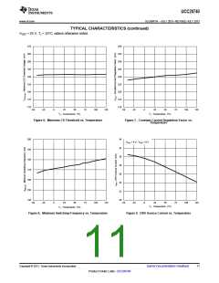
HV (High-Voltage Startup) The HV pin connects directly to the bulk capacitor to provide a startup current to the
VDD capacitor. The typical startup current is approximately 250 µA which provides fast charging of the
VDD capacitor. The internal HV startup device is active until VVDD exceeds the turnon UVLO threshold of
21 V at which time the HV startup device turns off. In the off state the HV leakage current is very low to
minimize standby losses of the controller. When VVDD falls below the 7.75 V UVLO turnoff threshold the
HV startup device turns on.
VS (Voltage Sense) The VS pin connects to a resistor-divider from the auxiliary winding to ground. The auxiliary
voltage waveform is sampled at the end of the transformer secondary-current demagnetization time to
provide accurate control of the output current when in constant-current mode. The waveform on the VS
pin determines the timing information to achieve valley-switching, and the timing to control the duty-cycle
of the transformer secondary current. Avoid placing a filter capacitor on this input which interferes with
accurate sensing of this waveform.
During the MOSFET on-time, this pin also senses VS current generated through RS1 by the reflected bulk-
capacitor voltage to provide for AC-input run and stop thresholds, and to compensate the current-sense
threshold across the AC-input range. For the AC-input run/stop function, the run threshold on VS is 225
µA and the stop threshold is 80 µA.
At the end of off-time demagnetization, the reflected output voltage is sampled at this pin to provide output
overvoltage protection. The values for the auxiliary voltage-divider upper-resistor, RS1, and lower-resistor,
RS2, are determined by Equation 1 and Equation 2.
where
•
•
NPA is the transformer primary-to-auxiliary turns-ratio,
VIN(run) is the AC RMS voltage to enable turnon of the controller (run),
(in case of DC input, leave out the √2 term in the equation),
•
IVSL(run) is the run-threshold for the current pulled out of the VS pin during the switch on-time (see
ELECTRICAL CHARACTERISTICS).
(1)
where
•
•
•
•
•
VOV is the maximum allowable peak voltage at the converter output,
VF is the output-rectifier forward drop at near-zero current,
NAS is the transformer auxiliary-to-secondary turns-ratio,
RS1 is the VS divider high-side resistance,
VOVP is the overvoltage detection threshold at the VS input (see ELECTRICAL CHARACTERISTICS).
(2)
8
Submit Documentation Feedback
Copyright © 2013, Texas Instruments Incorporated
Product Folder Links: UCC28740

 TI [ TEXAS INSTRUMENTS ]