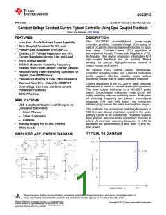
UCC28740
SLUSBF3A –JULY 2013–REVISED JULY 2013
www.ti.com
This integrated circuit can be damaged by ESD. Texas Instruments recommends that all integrated circuits be handled with
appropriate precautions. Failure to observe proper handling and installation procedures can cause damage.
ESD damage can range from subtle performance degradation to complete device failure. Precision integrated circuits may be more
susceptible to damage because very small parametric changes could cause the device not to meet its published specifications.
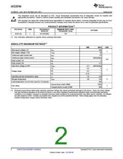
PRODUCT INFORMATION(1)
PACKAGE
PINS
ORDERABLE
DEVICES
MINIMUM SWITCHING
FREQUENCY (Hz)
OPTIONS
SOIC (D)
7
UCC28740D
170
(1) See Orderable Addendum for specific device ordering information.
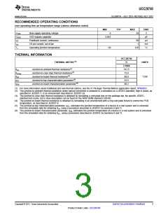
ABSOLUTE MAXIMUM RATINGS(1)
MIN
MAX
700
38
UNIT
Start-up pin voltage, HV
Bias supply voltage, VDD
Continuous gate-current sink
Continuous gate-current source
Peak current, VS
VHV
VVDD
IDRV
IDRV
IFB
V
50
Self-limiting
mA
V
1
Peak current, FB
IVS
−1.2
Gate-drive voltage at DRV
VDRV
CS
−0.5
−0.5
−0.5
−0.75
−55
Self-limiting
5
7
Voltage range
FB
VS
7
Operating junction temperature range
Storage temperature
TJ
150
150
260
2000
500
TSTG
−65
°C
V
Lead temperature 0.6 mm from case for 10 seconds
Human-body model (HBM)
ESD rating
Charged-device model (CDM)
(1) Stresses beyond those listed under absolute maximum ratings may cause permanent damage to the device. These are stress ratings
only and functional operation of the device at these or any other conditions beyond those indicated under recommended operating
conditions is not implied. Exposure to absolute-maximum-rated conditions for extended periods may affect device reliability. All voltages
are with respect to GND. Currents are positive into, negative out of the specified terminal. These ratings apply over the operating
ambient temperature ranges unless otherwise noted.
2
Submit Documentation Feedback
Copyright © 2013, Texas Instruments Incorporated
Product Folder Links: UCC28740

 TI [ TEXAS INSTRUMENTS ]