UCC28070-Q1
SLUSA71A –JULY 2010–REVISED JUNE 2011
www.ti.com
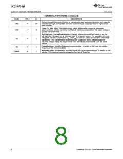
TERMINAL FUNCTIONS (continued)
NAME
PIN #
I/O
DESCRIPTION
Device Ground Reference. Connect all compensation and programming resistor and capacitor
networks to this pin. Connect this pin to the system through a separate trace for high-current
noise isolation.
GND
16
I/O
Phase B's Gate Drive. This limited-current output is intended to connect to a separate
gate-drivedevice suitable for driving the Phase B switching component(s). The output voltage is
typically clamped to 13.5 V.
GDB
SS
17
18
O
I
Soft-Start and External Fault Interface. Connect a capacitor to GND on this pin to set the
soft-start slew rate based on an internally-fixed 10-μA current source. The regulation reference
voltage for VSENSE is clamped to VSS until VSS exceeds 3 V. Upon recovery from certain fault
conditions a 1-mA current source is present at the SS pin until the SS voltage equals the
VSENSE voltage. Pulling the SS pin below 0.6 V immediately disables both GDA and GDB
outputs.
Timing Resistor. Oscillator frequency programming pin. A resistor to GND sets the running
frequency of the internal oscillator.
RT
19
20
I
I
Maximum Duty-Cycle Resistor. Maximum PWM duty-cycle programming pin. A resistor to GND
DMAX
sets the PWM maximum duty-cycle based on the ratio of RDMX/RRT
.
8
Copyright © 2010–2011, Texas Instruments Incorporated

 TI [ TEXAS INSTRUMENTS ]