UCC28070-Q1
www.ti.com
SLUSA71A –JULY 2010–REVISED JUNE 2011
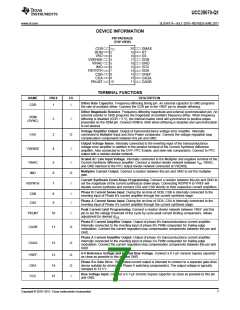
DEVICE INFORMATION
PW PACKAGE
(TOP VIEW)
1
20
19
18
17
16
15
14
13
12
11
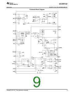
CDR
RDM
VAO
DMAX
RT
SS
2
3
4
VSENSE
VINAC
IMO
GDB
GND
VCC
GDA
VREF
CAOA
CAOB
5
6
7
RSYNTH
CSB
CSA
8
9
10
PKLMT
TERMINAL FUNCTIONS
NAME
PIN #
I/O
DESCRIPTION
Dither Rate Capacitor. Frequency-dithering timing pin. An external capacitor to GND programs
the rate of oscillator dither. Connect the CDR pin to the VREF pin to disable dithering.
CDR
1
I
Dither Magnitude Resistor. Frequency-dithering magnitude and external synchronization pin. An
external resistor to GND programs the magnitude of oscillator frequency dither. When frequency
dithering is disabled (CDR > 5 V), the internal master clock will synchronize to positive edges
presented on the RDM pin. Connect RDM to GND when dithering is disabled and synchronization
is not desired.
RDM
(SYNC)
2
I
Voltage Amplifier Output. Output of transconductance voltage error amplifier. Internally
connected to Multiplier input and Zero-Power comparator. Connect the voltage regulation loop
compensation components between this pin and GND.
VAO
3
4
O
I
Output Voltage Sense. Internally connected to the inverting input of the transconductance
voltage error amplifier in addition to the positive terminal of the Current Synthesis difference
amplifier. Also connected to the OVP, PFC Enable, and slew-rate comparators. Connect to PFC
output with a resistor-divider network.
VSENSE
Scaled AC Line Input Voltage. Internally connected to the Multiplier and negative terminal of the
Current Synthesis difference amplifier. Connect a resistor-divider network between VIN, VINAC,
and GND identical to the PFC output divider network connected at VSENSE.
VINAC
IMO
5
6
7
I
O
I
Multiplier Current Output. Connect a resistor between this pin and GND to set the multiplier
gain.
Current Synthesis Down-Slope Programming. Connect a resistor between this pin and GND to
set the magnitude of the current synthesizer down-slope. Connecting RSYNTH to VREF will
disable current synthesis and connect CSA and CSB directly to their respective current amplifiers.
RSYNTH
Phase B Current Sense Input. During the on-time of GDB, CSB is internally connected to the
inverting input of Phase B's current amplifier through the current synthesis stage.
CSB
CSA
8
9
I
I
Phase A Current Sense Input. During the on-time of GDA, CSA is internally connected to the
inverting input of Phase A's current amplifier through the current synthesis stage.
Peak Current Limit Programming. Connect a resistor-divider network between VREF and this
PKLMT
CAOB
10
11
I
pin to set the voltage threshold of the cycle-by-cycle peak current limiting comparators. Allows
adjustment for desired ΔILB
.
Phase B Current Amplifier Output. Output of phase B's transconductance current amplifier.
Internally connected to the inverting input of phase B's PWM comparator for trailing-edge
modulation. Connect the current regulation loop compensation components between this pin and
GND.
O
Phase A Current Amplifier Output. Output of phase A's transconductance current amplifier.
Internally connected to the inverting input of phase A's PWM comparator for trailing-edge
modulation. Connect the current regulation loop compensation components between this pin and
GND.
CAOA
12
O
6-V Reference Voltage and Internal Bias Voltage. Connect a 0.1-μF ceramic bypass capacitor
as close as possible to this pin and GND.
VREF
GDA
VCC
13
14
15
O
O
I
Phase A's Gate Drive. This limited-current output is intended to connect to a separate gate-drive
device suitable for driving the Phase A switching component(s). The output voltage is typically
clamped to 13.5 V.
Bias Voltage Input. Connect a 0.1-μF ceramic bypass capacitor as close as possible to this pin
and GND.
Copyright © 2010–2011, Texas Instruments Incorporated
7

 TI [ TEXAS INSTRUMENTS ]