UCC28070-Q1
SLUSA71A –JULY 2010–REVISED JUNE 2011
www.ti.com
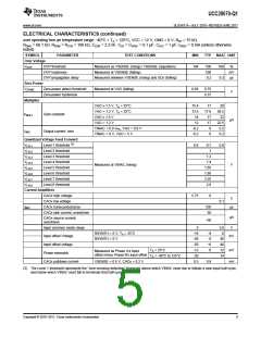
ELECTRICAL CHARACTERISTICS (continued)
over operating free-air temperature range −40°C < TA < 125°C, VCC = 12 V, GND = 0 V, RRT = 75 kΩ,
RDMX = 68.1 kΩ, RRDM = RSYN = 100 kΩ, CCDR = 2.2 nF, CSS = CVREF = 0.1 µF, CVCC = 1 µF, IVREF = 0 mA (unless otherwise
noted)
SYMBOL
Clock Synchronization
VCDR SYNC enable threshold
PARAMETER
TEST CONDITIONS
MIN
TYP
MAX UNIT
Measured at CDR (rising)
5
50
5.25
100
1.5
V
SYNC propagation delay
SYNC threshold (Rising)
SYNC threshold (Falling)
VCDR = 6 V, Measured from RDM (rising) to GDx (rising)
VCDR = 6 V, Measured at RDM
ns
1.2
0.7
V
VCDR = 6 V, Measured at RDM
0.4
0.2
Positive pulse width
μs
SYNC pulses
(2)
Maximum duty cycle
50
%
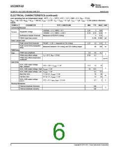
Voltage Amplifier
VSENSE voltage
In regulation, TA = 25°C
In regulation
2.94
2.84
3
3
3.06
3.10
500
5.2
V
nA
V
VSENSE voltage
VSENSE input bias current
VAO high voltage
In regulation
250
5
VSENSE = 2.9 V
4.8
VAO low voltage
VSENSE = 3.1 V
0.05
70
0.50
gMV
VAO transconductance
2.8 V < VSENSE < 3.2 V, VAO = 3 V
μs
VAO sink current, overdriven
limit
VSENSE = 3.5 V, VAO = 3 V
30
−30
VAO source current, overdriven VSENSE = 2.5 V, VAO = 3 V, SS = 3 V
μA
VAO source current,
VSENSE = 2.5 V, VAO = 3 V
overdriven limit + ISRC
−130
Slew-rate correction threshold
Measured as VSENSE (falling) / VSENSE (regulation)
92
93
3
95
9
%
mV
μA
Slew-rate correction hysteresis Measured at VSENSE (rising)
ISRC
Slew-rate correction current
Measured at VAO, in addition to VAO source current.
−100
Slew-rate correction enable
threshold
Measured at SS (rising)
4
V
VAO discharge current
VSENSE = 0.5 V, VAO = 1 V
10
μA
Soft Start
ISS
SS source current
Adaptive source current
Adaptive SS disable
SS sink current
VSENSE = 0.9 V, SS = 1 V
VSENSE = 2.0 V, SS = 1 V
Measured as VSENSE – SS
VSENSE = 0.5 V, SS = 0.2 V
−10
−1.5
0
μA
-2.5 mA
30 mV
mA
-30
0.5
0.9
(2) Due to the influence of the synchronization pulse width on the programmability of the maximum PWM switching duty cycle (DMAX) it is
recommended to minimize the synchronization signal's duty cycle.
4
Copyright © 2010–2011, Texas Instruments Incorporated

 TI [ TEXAS INSTRUMENTS ]